6.15 Fan Speed Control And Monitoring
The LPC47M45x may control the speed of one fan as well as monitor it if it is equipped with a fan tachometer output.
The following sections will clarify how this chip controls the speed of a fan and its’ monitoring capabilities.
6.15.1 FAN SPEED CONTROL
The fan speed control for the LPC47M45x is implemented as pulse width modulators with fan clock speed selection.
There is one signal pin, FAN (located on pin 58), dedicated to controlling the speeds of a fan. This signal is
controlled by the Runtime registers FAN and Fan Control that are described below (see also section 8 Runtime
Registers on page 156 ).
Note: The fan control pin comes up as an output and is low following a VCC POR and PCI Reset. This pin may not
be used for wakeup events under VTR power (VCC=0).
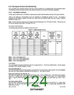
Fan Speed Control Summary
The following table illustrates the different modes for the fan.
Table 61 – Different Modes for Fan
FAN
FAN
FAN
6-BIT DUTY
CYCLE
FAN
CLOCK
SOURCE
SELECT
BIT
CLOCK
CONTROL MULTIPLIER
CLOCK
CLOCK
SELECT
BIT
DUTY
CYCLE
(%)
CONTROL
BITS[6:1]
FOUT
BIT
BIT
(NOTE 4)
(NOTE 1)
(NOTE 2)
(DCC)
(NOTE 3)
0
X
0
0
0
0
1
1
1
1
X
X
X
0Hz – LOW
15.625kHz
23.438kHz
40Hz
0
-
0
0
0
0
0
0
0
0
1
0
0
1
1
0
0
1
1
X
0
1
0
1
0
1
0
1
X
1-63
(DCC/64)
100
60Hz
31.25kHz
46.876kHz
80Hz
120Hz
0Hz – HIGH
-
-
Note 1: This is FAN Register Bit 0
Note 2: This is Fan Control Register Bit 2
Note 3: This is Fan Control Register Bit 0
Note 4: This is FAN Register Bit 7
FAN Register
The FAN Register is located at 0x56 from base I/O in Logical Device A. The bits are defined below. See the register
description in the “Runtime Registers” section.
Fan Clock Select Bit, D7
The Fan Clock select bit in the FAN registers is used with the Fan Clock Source Select and the Fan Clock Multiplier
bits in the Fan Control register to determine the fan speed FOUT. See Table 61 above.
Duty Cycle Control for Fan, Bits D6 – D1
The Duty Cycle Control (DCC) bits determine the fan duty cycle. The LPC47M45x has ≈1.56% duty cycle resolution.
When DCC = “000000” (min. value), FOUT is always low. When DCC is “111111” (max. value), FOUT is almost always
high; i.e., high for 63/64th and low for 1/64th of the FOUT period. Generally, the FOUT duty cycle (%) is (DCC ÷ 64) ×
100.
Fan Clock Control, Bit D0
The Fan Clock Control bit D0 is used to override the Duty Cycle Control for Fan bits and force FOUT always high.
When D0 = “0”, the DCC bits determine the FOUT duty cycle. When D0 = 1, FOUT is always high, regardless of the
state of the DCC bits.
SMSC LPC47S45x
Page 124 of 259
Rev. 06-01-06
DATASHEET

 SMSC [ SMSC CORPORATION ]