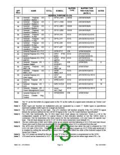
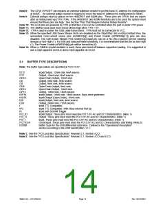
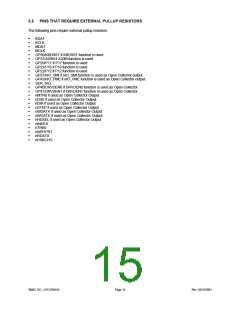
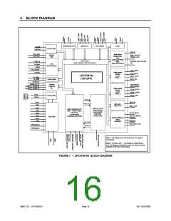
5
POWER FUNCTIONALITY
The LPC47M14x has three power planes: VCC, VTR, and VREF.
5.1 VCC POWER
The LPC47M14x is a 3.3 Volt part. The VCC supply is 3.3 Volts (nominal). See the “Operational Description” Section
and the “Maximum Current Values” subsection.
5.1.1
3 Volt Operation / 5 Volt Tolerance
The LPC47M14x is a 3.3 Volt part. It is intended solely for 3.3V applications. All signal pins are 5V tolerant except
those that pertain to the LPC Bus and USB Hub interfaces; that is, the input voltage is 5.5V max, and the I/O buffer
output pads are backdrive protected.
The LPC interface pins are 3.3 V only. These signals meet PCI DC specifications for 3.3V signaling. These pins are:
ꢀ
ꢀ
ꢀ
ꢀ
LAD[3:0]
LFRAME#
LDRQ#
LPCPD#
The USB interface pins are 3.3V tolerant. The maximum input voltage tolerated on the downstream port pins is 3.6V
(See “Operational Description” for the IOUSB buffers). These pins are labeled:
ꢀ
ꢀ
PD+[1:4]
PD-[1:4]
The input voltage for all other pins is 5.5V max including the following pins:
ꢀ
ꢀ
ꢀ
ꢀ
ꢀ
ꢀ
PCI_RESET#
PCI_CLK
SER_IRQ
nIO_PME
nUSBOC[1:4]
nPWREN[1:4]
5.2 USB POWER
The LPC47M14x requires that the USB Hub maintain power for wake-up events in the absence of VCC power. To
meet these requirements, the Hub Block and the transceiver pins are powered by VTR. CLKI32, which is also
powered by VTR, is used to monitor changes in the signaling on the USB ports. This will enable the Hub Block to
resume from a suspend state by receiving a signal on either its downstream ports or its upstream port.
5.3 VTR SUPPORT
The LPC47M14x requires a trickle supply (VTR) to provide sleep current for the programmable wake-up events in the
PME interface when VCC is removed. The VTR pin is connected to the VTR (standby) power supply, which is 3.3
Volts (nominal). See the “Operational Description” Section. The maximum VTR current that is required depends on
the functions that are used in the part. See “Trickle Power Functionality” subsection and “Maximum Current Values”
subsection. This voltage source is also used to power the USB Hub interface, the IR interface, the PME configuration
registers, and the PME interface. The VTR pin generates a VTR Power-on-Reset signal to initialize these components.
Note: If VTR is to be used for programmable wake-up events when VCC is removed, VTR must be at its full
minimum potential at least 10 µs before Vcc begins a power-on cycle. When VTR and Vcc are fully
powered, the potential difference between the two supplies must not exceed 500mV.
5.4 VREF PIN
The LPC47M14x has a reference voltage pin input on pin 44 of the part. This reference voltage can be connected to
either a 5V supply or a 3.3V supply. It is used for the game port. See the “GAME PORT LOGIC” section.
SMSC DS – LPC47M14X
Page 17
Rev. 03/19/2001

 SMSC [ SMSC CORPORATION ]