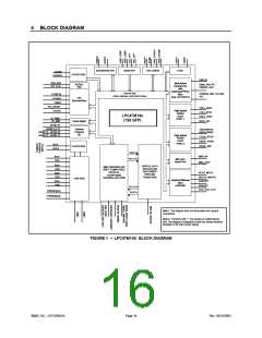
6
FUNCTIONAL DESCRIPTION
6.1
SUPER I/O REGISTERS
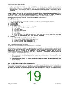
The address map, shown below in Table 1 shows the addresses of the different blocks of the Super I/O immediately
after power up. The base addresses of the FDC, serial and parallel ports, PME register block, Game port and
configuration register block can be moved via the configuration registers. Some addresses are used to access more
than one register.
6.2 HOST PROCESSOR INTERFACE (LPC)
The host processor communicates with the LPC47M14x through a series of read/write registers via the LPC interface.
The port addresses for these registers are shown in Table 1. Register access is accomplished through I/O cycles or
DMA transfers. All registers are 8 bits wide.
Table 1 – Super I/O Block Addresses
LOGICAL
ADDRESS
BLOCK NAME
NOTES
DEVICE
Base+(0-5) and +(7)
Base+(0-7)
Floppy Disk
Serial Port Com 1
Serial Port Com 2
0
4
5
Base1+(0-7)
Base2+(0-7)
Parallel Port
SPP
3
Base+(0-3)
Base+(0-7)
EPP
Base+(0-3), +(400-402)
Base+(0-7), +(400-402)
60, 64
ECP
ECP+EPP+SPP
KYBD
7
9
A
B
Base + 0
Game Port
Runtime Registers
MPU-401
Configuration
USB Hub
Base + (0-5F)
Base + (0-1)
Base + (0-1)
n/a
2
1
C
Note: Refer to the configuration register descriptions for setting the base address.
Note 1: No Addressable Registers in the Hub Block.
Note 2: Logical Device A is referred to as the Runtime Register block or PME Block and may be
used interchangeably throughout this document.
SMSC DS – LPC47M14X
Page 20
Rev. 03/19/2001

 SMSC [ SMSC CORPORATION ]