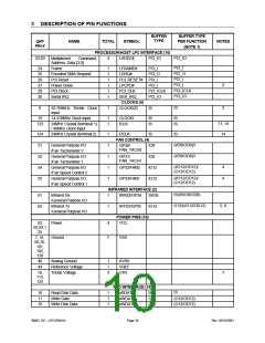
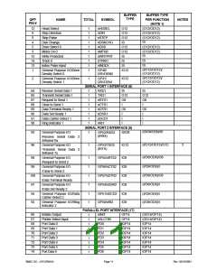
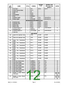
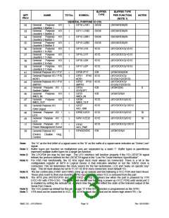
Note 8: The GP24 /SYSOPT pin requires an external pulldown resistor to put the base IO address for configuration
at 0x02E. An external pullup resistor is required to move the base IO address for configuration to 0x04E.
Note 9: External pullups must be placed on the nKBDRST and A20M pins. These pins are GPIOs that are inputs
after an initial power-up (VTR POR). If the nKBDRST and A20M functions are to be used the system must
ensure that these pins are high. See Section “Pins That Require External Pullup Resistor”.
Note 10: The LED pins are powered by VTR so that the LEDs can be controlled when the part is under VTR power.
Note 11: The 48MHz clock input must not be driven high when VTR = 0V.
Note 12: VTR is used to power the USB cable transceivers. VTR must not be connected to VCC.
Note 13: When the specified USB Down Stream Ports are disabled via the Strp0/Strp1 bit or nStrp1/nStrp0 Pins, the
associated Over-current sense pins (nUSBOC[x]) and Power Enable (nPWREN[4:1]) pins are also
disabled. The USB Down Stream Port nUSBOC[x] input pin can be a NC (No Connect) pin for existing
designs or tied High (1). For EMI and reduced Noise sensitivity, it is recommended that the pin be tied High
(1). The Power Enable (nPWREN[x]) pin will be forced low (0).
Note 14: When a 24MHz crystal oscillator is used, these pins need off-balance capacitive loading. It is suggested to
use a 22pf capacitor on ICLK and a 10pf capacitor on OCLK.
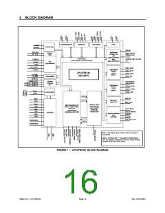
3.1 BUFFER TYPE DESCRIPTIONS
Note: The buffer type values are specified at VCC=3.3V
IO12
O12
Input/Output, 12mA sink, 6mA source.
Output, 12mA sink, 6mA source.
OD12
O6
Open Drain Output, 12mA sink.
Output, 6mA sink, 3mA source.
O8
Output, 8mA sink, 4mA source.
OD8
OD14
OP14
IOP14
IOD16
IO8
Open Drain Output, 8mA sink.
Open Drain Output, 14mA sink.
Output, 14mA sink, 14mA source.
Input/Output, 14mA sink, 14mA source. Back-drive protected.
Input/Output (Open Drain), 16mA sink.
Input/Output, 8mA sink, 4mA source.
O24
Output, 24mA sink, 12mA source.
I
Input TTL Compatible.
IPU
Input TTL Compatible. With 30ua internal Pull Up
Input with Schmitt Trigger.
IS
PCI_IO
PCI_O
PCI_I
PCI_ICLK
IOUSB
Input/Output. These pins must meet the PCI 3.3V AC and DC Characteristics. (Note 1)
Output. These pins must meet the PCI 3.3V AC and DC Characteristics. (Note 1)
Input. These pins must meet the PCI 3.3V AC and DC Characteristics. (Note 1)
Clock Input. These pins must meet the PCI 3.3V AC and DC Characteristics and timing. (Note 2)
Buffer Type for the USB differential data lines. Defined in the “Operational Description”
section according to the USB specification; V1.1
Note 1: See the “PCI Local Bus Specification,” Revision 2.1, Section 4.2.2.
Note 2: See the “PCI Local Bus Specification,” Revision 2.1, Section 4.2.2 and 4.2.3.
SMSC DS – LPC47M14X
Page 14
Rev. 03/19/2001

 SMSC [ SMSC CORPORATION ]