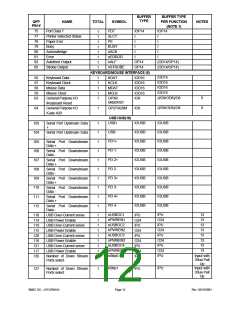
4
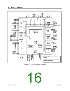
BLOCK DIAGRAM
2nd Infrared Port
Game Port
Fan Control
LEDs
CLK32
CLOCKI
CLOCK GEN
PD[7,0]
SER_IRQ
PCI_CLK
Multi-Mode
Parallel Port
with
SERIAL
IRQ
Busy, Slct, PE,
ERROR, ACK
ChiProtectTM/FDC
MUX
Internal Bus
STROBE, INIT, SLCTIN,
ALF
LAD[3:0]
LFrame
(Data, Address, and Control lines)
(see LPC47B27x)
LPC
Bus Interface
LDRQ
PCI_RESET
LPCPD
TXD1, RXD1
CTS1, RTS1
DSR1, DTR1
DCD1, RI1
High-Speed
16550A
LPC47M14x
(128 QFP)
UART
IO_PME*
IO_SMI*
GP1[0:7]*
GP2[0:2,4:7]*
PORT 1
Power Mgmt
General
Purpose
I/O
TXD2 (IRTX)*,
RXD2 (IRRX)*
GP3[0:7]*, GP4[0:3]*
GP5[0:7]*, GP6[0:1]*
High-Speed
16550A
CTS2*, RTS2 *
DSR2*, DTR2*
DCD2*, RI2*
UART
PORT 2
ICLK
OCLK
CLOCK GEN
WDATA
MIDI_IN*
PD1+
PD1-
WCLOCK
MPU-401
Serial Port
MIDI_OUT*
PD2+
PD2-
DIGITAL DATA
SEPARATOR
WITH WRITE
PRECOM-
SMC PROPRIETARY
82077 COMPATIBLE
VERTICAL
KCLK, MCLK
PD3+
PD3-
PD4+
PD4-
FLOPPYDISK
PENSATION
KDATA, MDATA
GateA20*
CONTROLLER CORE
USB HUB
Keyboard/Mouse
8042
controller
KRESET*
P12*, P16*, P17*
RCLOCK
RDATA
PWROK[3,0]
PWREN[3,0]
Note 1: This diagram does not show power and ground
connections.
Note 2: Functions with "*" are located on multifunctional
pins. This diagram is designed to show the various functions
available on the chip (not pin layout).
FIGURE 1 – LPC47M14X BLOCK DIAGRAM
SMSC DS – LPC47M14X
Page 16
Rev. 03/19/2001

 SMSC [ SMSC CORPORATION ]