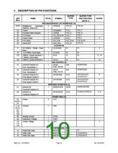
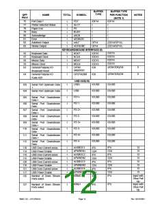
BUFFER
TYPE
BUFFER TYPE
PER FUNCTION
(NOTE 1)
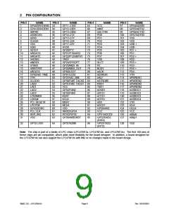
QFP
NAME
TOTAL
SYMBOL
NOTES
PIN #
GENERAL PURPOSE I/O (19)
General
Purpose
I/O
I/O
I/O
I/O
I/O
I/O
I/O
I/O
GP10 /J1B1
GP11 /J1B2
GP12 /J2B1
GP13 /J2B2
GP14 /J1X
GP15 /J1Y
GP16 /J2X
GP17 /J2Y
GP20 /P17
IS/O8
IS/O8
IS/O8
IS/O8
IO12
IO12
IO12
IO12
IO8
(IS/O8/OD8)/IS
32
33
34
35
36
37
38
39
1
1
1
1
1
1
1
1
/Joystick 1 Button 1
General
/Joystick 1 Button 2
General Purpose
/Joystick 2 Button 1
General Purpose
/Joystick 2 Button 2
General Purpose
Purpose
(IS/O8/OD8)/IS
(IS/O8/OD8)/IS
(IS/O8/OD8)/IS
(I/O12/OD12)/ IO12
(I/O12/OD12)/ IO12
(I/O12/OD12)/ IO12
(I/O12/OD12)/ IO12
(I/O8/OD8)/IO8
(I/O12/OD12)/
IO12/(O12/OD12)
(I/O12/OD12)/
IO12/(O12/OD12)
(I/O8/OD8)
/Joystick 1 X-Axis
General
Purpose
/Joystick 1 Y-Axis
General
Purpose
/Joystick 2 X-Axis
General
Purpose
/Joystick 2 Y-Axis
General Purpose I/O / P17
41
42
1
1
General Purpose I/O / P16
GP21 /P16/ IO12
/nDS1
nDS1
General Purpose I/O / P12
/nMTR1
GP22 /P12/ IO12
nMTR1
43
45
46
47
50
1
1
1
1
1
General Purpose I/O
System Option
/
GP24
IO8
8
/SYSOPT
GP25
General
Purpose
I/O
I/O
IO8
(I/O8/OD8)/I
/MIDI_IN
General
/MIDI_IN
GP26
Purpose
IO12
IO12
(I/O12/OD12)/O12
(I/O12/OD12)/ OD12
/MIDI_OUT
/MIDI_OUT
General Purpose I/O
/SMI Output
General Purpose I/O
GP27
/nIO_SMI
/
/
/
GP60 /LED1
IO12
IO12
IO12
(I/O12/OD12)/O12
(I/O12/OD12)/O12
(I/O12/OD12)/ OD12
10
10
48
49
17
1
1
1
LED
General Purpose I/O
LED
GP61 /LED2
General Purpose I/O
GP42
Power Management Event
General Purpose I/O
/nIO_PME
GP43/DDRC
IO8
(I/O8/OD8)/I
28
1
/Device
Disable
Reg.
Control
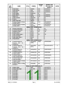
Note:
The "n" as the first letter of a signal name or the “#” as the suffix of a signal name indicates an "Active Low"
signal.
Note 1: Buffer types per function on multiplexed pins are separated by a slash “/”. Buffer types in parenthesis
represent multiple buffer types for a single pin function.
Note 2: The LPCPD# pin may be tied high. The LPC interface will function properly if the PCI_RESET# signal
follows the protocol defined for the LRESET# signal in the “Low Pin Count Interface Specification”.
Note 3: For USB Hub functionality, the 32 KHz input clock must always be connected. There is a bit in the
configuration register at 0xF0 in Logical Device A that indicates whether or not the 32KHz clock is
connected. This bit determines the clock source for the fan tachometer, LED and “wake on specific key”
logic. This bit must always be set to ‘0’ (‘0’=32 KHz clock connected; reset default=‘0’).
Note 4: The fan control pins (FAN1 and FAN2) come up as outputs and low following a VCC POR and Hard Reset.
These pins revert to their non-inverting GPIO input function when VCC is removed from the part.
Note 5: The IRTX pins (IRTX2/GP35 and GP53/TXD2 (IRTX)) are driven low when the part is powered by VTR
(VCC=0V with VTR=3.3V). These pins will remain low following a power-up (VCC POR) until serial port 2
is enabled by setting the activate bit, at which time the pin will reflect the state of the transmit output of the
Serial Port 2 block.
Note 6: The VCC power-up default for this pin is Logic “0” if the IRTX function is programmed on the GPIO.
Note 7: VTR must not be connected to VCC. The 32 KHz input clock must not be driven high whenVTR = 0v.
SMSC DS – LPC47M14X
Page 13
Rev. 03/19/2001

 SMSC [ SMSC CORPORATION ]