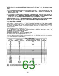
Following a VTR POR, the IRTX and IRTX2 pins will be output and low. They will remain low until one of the
following conditions are met:
IRTX2/GP35 Pin. This pin defaults to the IRTX2 function.
1. This pin will remain low following a VCC POR until serial port 2 is enabled by setting the activate bit, at which
time the pin will reflect the state of the IR transmit output of the Serial Port 2 block.
2. This pin will remain low following a VCC POR until the GPIO output function is selected for the pin, at which time
the pin will reflect the state of the GPIO data bit if it is configured as an output.
GP53/TXD2 (IRTX) Pin. This pin defaults to the GPIO output function.
1. This pin will remain low following a VCC POR until the TXD2 function is selected for the pin AND serial port 2 is
enabled by setting the activate bit, at which time the pin will reflect the state of the transmit output of serial port 2.
Following a VCC POR, setting the TXD2_MODE bit (bit 5 in Serial Port 2 Mode Register, 0xF0 in Logical Device
5 Configuration Registers) to ‘1’ will change the state of the TXD2 pin from low to tristate, regardless of the
function selected on the pin (GP10 or TXD2), regardless of the state of the activate bit for serial port 2 and
regardless of the state of VCC. When VCC is removed from the part while the TXD2_MODE bit is set to ‘1’, the
TXD2 pin will remain tristate unless a VTR POR occurs, which will reset the TXD2_MODE bit.
2. This pin will remain low following a VCC POR until the corresponding GPIO data bit (GP5 register bit 3) is set or
the polarity bit in the GP53 control register is set.
The TXD2_MODE bit is implemented for modems that do not assert the ring indicator pin when TXD2 is sensed low. If
required, this bit should be used as follows:
•
•
When the activate bit for serial port 2 is cleared prior to entering a sleep state, set the TXD2_MODE bit.
When the activate bit for serial port 2 is set, upon exiting a sleep state, clear the TXD2_MODE bit.
The IRTX2 pin is not affected by the TXD2_MODE bit.
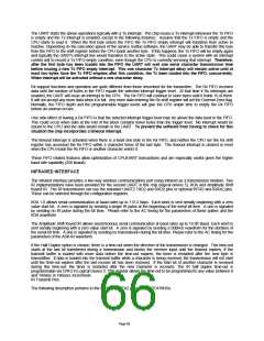
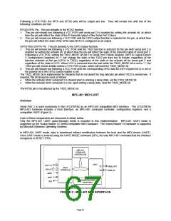
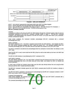
MPU-401 MIDI UART
Overview
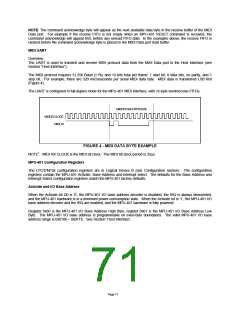
Serial Port 3 is used exclusively in the LPC47M10x as an MPU-401-compatible MIDI Interface. The LPC47M10x
MPU-401 hardware includes a Host Interface, an MPU-401 command controller, configuration registers, and a
compatible UART (Figure 2).
Each of these components are discussed in detail, below.
Only the MPU-401 UART (pass-through) mode is included in this implementation. MPU-401 UART mode is
supported on the Sound Blaster 16 Series-compatible MIDI hardware. The Sound Blaster 16 hardware is supported
by Microsoft Windows Operating Systems.
In MPU-401 UART mode, data is transferred without modification between the host and the MIDI device (UART).
Once UART mode is entered using the UART MODE command (3Fh), the only MPU-401 command that the interface
recognizes is RESET (FFh).
MPU-401
COMMAND
CONTROLLER
UART
SA[15:0]
TX
RX
MIDI_OUT
MIDI_IN
HOST
INTERFACE
SD[7:0]
nIOW
nIOR
IRQ
CONFIGURATION
REGISTERS
FIGURE 2 - MPU-401 MIDI INTERFACE
Page 67

 SMSC [ SMSC CORPORATION ]