*DLAB is Bit 7 of the Line Control Register (ADDR = 3).
Note 1: Bit 0 is the least significant bit. It is the first bit serially transmitted or received.
Note 2: When operating in the XT mode, this bit will be set any time that the transmitter shift register is empty.
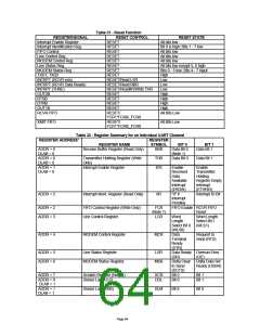
Table 32 - Register Summary for an Individual UART Channel (continued)
BIT 2
Data Bit 2
Data Bit 2
Enable
BIT 3
Data Bit 3
Data Bit 3
Enable
BIT 4
Data Bit 4
Data Bit 4
0
BIT 5
Data Bit 5
Data Bit 5
0
BIT 6
Data Bit 6
Data Bit 6
0
BIT 7
Data Bit 7
Data Bit 7
0
Receiver Line MODEM
Status
Status
Interrupt
(ELSI)
Interrupt
(EMSI)
Interrupt ID Bit Interrupt ID Bit
(Note 5)
0
0
FIFOs
Enabled
(Note 5)
FIFOs
Enabled
(Note 5)
XMIT FIFO
Reset
DMA Mode
Select (Note
6)
Parity Enable Even Parity
(PEN)
Reserved
Reserved
Stick Parity
0
RCVR Trigger RCVR Trigger
LSB
MSB
Number of
Stop Bits
(STB)
Set Break
Divisor Latch
Access Bit
(DLAB)
0
Select (EPS)
OUT1
OUT2
Loop
0
(Note 3)
Parity Error
(PE)
(Note 3)
Framing Error Break
(FE) Interrupt (BI)
Transmitter
Holding
Register
Transmitter
Empty (TEMT) FIFO (Note 5)
(Note 2)
Error in RCVR
(THRE)
Trailing Edge Delta Data
Clear to Send Data Set
Ring Indicator Data Carrier
Ring Indicator Carrier Detect (CTS)
Ready (DSR) (RI)
Detect (DCD)
(TERI)
(DDCD)
Bit 2
Bit 2
Bit 10
Bit 3
Bit 3
Bit 11
Bit 4
Bit 4
Bit 12
Bit 5
Bit 5
Bit 13
Bit 6
Bit 6
Bit 14
Bit 7
Bit 7
Bit 15
Note 3: This bit no longer has a pin associated with it.
Note 4: When operating in the XT mode, this register is not available.
Note 5: These bits are always zero in the non-FIFO mode.
Note 6: Writing a one to this bit has no effect. DMA modes are not supported in this chip.
Note 7: The UART1 and UART2 FCR’s are shadowed in the UART1 FIFO Control Shadow Register (runtime
register at offset 0x20) and UART2 FIFO Control Shadow Register (runtime register at offset 0x21).
NOTES ON SERIAL PORT OPERATION
FIFO MODE OPERATION:
GENERAL
The RCVR FIFO will hold up to 16 bytes regardless of which trigger level is selected.
TX AND RX FIFO OPERATION
The Tx portion of the UART transmits data through TXD as soon as the CPU loads a byte into the Tx FIFO. The UART
will prevent loads to the Tx FIFO if it currently holds 16 characters. Loading to the Tx FIFO will again be enabled
as soon as the next character is transferred to the Tx shift register. These capabilities account for the largely
autonomous operation of the Tx.
Page 65

 SMSC [ SMSC CORPORATION ]