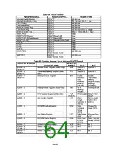
Table 31 - Reset Function
RESET CONTROL
RESET
REGISTER/SIGNAL
Interrupt Enable Register
RESET STATE
All bits low
Interrupt Identification Reg.
FIFO Control
RESET
RESET
Bit 0 is high; Bits 1 - 7 low
All bits low
Line Control Reg.
MODEM Control Reg.
Line Status Reg.
MODEM Status Reg.
TXD1, TXD2
RESET
RESET
RESET
RESET
All bits low
All bits low
All bits low except 5, 6 high
Bits 0 - 3 low; Bits 4 - 7 input
RESET
High
INTRPT (RCVR errs)
INTRPT (RCVR Data Ready)
INTRPT (THRE)
OUT2B
RESET/Read LSR
RESET/Read RBR
RESET/ReadIIR/Write THR
RESET
Low
Low
Low
High
RTSB
RESET
High
DTRB
RESET
High
OUT1B
RESET
High
RCVR FIFO
RESET/
All Bits Low
FCR1*FCR0/_FCR0
XMIT FIFO
RESET/
All Bits Low
FCR1*FCR0/_FCR0
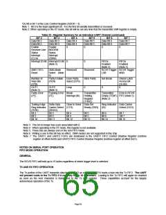
Table 32 - Register Summary for an Individual UART Channel
REGISTER ADDRESS*
REGISTER
SYMBOL
RBR
REGISTER NAME
Receive Buffer Register (Read Only)
BIT 0
Data Bit 0
(Note 1)
BIT 1
Data Bit 1
ADDR = 0
DLAB = 0
ADDR = 0
DLAB = 0
ADDR = 1
DLAB = 0
Transmitter Holding Register (Write
Only)
Interrupt Enable Register
THR
IER
Data Bit 0
Data Bit 1
Enable
Received
Data
Enable
Transmitter
Holding
Available
Interrupt
(ERDAI)
"0" if
Register Empty
Interrupt
(ETHREI)
ADDR = 2
Interrupt Ident. Register (Read Only)
IIR
Interrupt ID Bit
Interrupt
Pending
ADDR = 2
ADDR = 3
FIFO Control Register (Write Only)
Line Control Register
FCR
(Note 7)
LCR
FIFO Enable RCVR FIFO
Reset
Word
Word Length
Select Bit 1
Length
Select Bit 0 (WLS1)
(WLS0)
ADDR = 4
MODEM Control Register
MCR
Data
Request to
Send (RTS)
Terminal
Ready
(DTR)
ADDR = 5
ADDR = 6
Line Status Register
LSR
Data Ready Overrun Error
(DR)
(OE)
MODEM Status Register
MSR
Delta Clear
to Send
(DCTS)
Bit 0
Delta Data Set
Ready (DDSR)
ADDR = 7
ADDR = 0
DLAB = 1
ADDR = 1
DLAB = 1
Scratch Register (Note 4)
Divisor Latch (LS)
SCR
DDL
Bit 1
Bit 1
Bit 0
Divisor Latch (MS)
DLM
Bit 8
Bit 9
Page 64

 SMSC [ SMSC CORPORATION ]