SCRATCHPAD REGISTER (SCR)
Address Offset =7H, DLAB =X, READ/WRITE
This 8 bit read/write register has no effect on the operation of the Serial Port. It is intended as a scratchpad register to
be used by the programmer to hold data temporarily.
PROGRAMMABLE BAUD RATE GENERATOR (AND DIVISOR LATCHES DLH, DLL)
The Serial Port contains a programmable Baud Rate Generator that is capable of dividing the PLL clock by any
divisor from 1 to 65535. The internal PLL clock is divided down to generate a 1.8462MHz frequency for Baud Rates
less than 38.4k, a 1.8432MHz frequency for 115.2k, a 3.6864MHz frequency for 230.4k and a 7.3728MHz frequency
for 460.8k. This output frequency of the Baud Rate Generator is 16x the Baud rate. Two 8 bit latches store the
divisor in 16 bit binary format. These Divisor Latches must be loaded during initialization in order to insure desired
operation of the Baud Rate Generator. Upon loading either of the Divisor Latches, a 16 bit Baud counter is
immediately loaded. This prevents long counts on initial load. If a 0 is loaded into the BRG registers the output
divides the clock by the number 3. If a 1 is loaded the output is the inverse of the input oscillator. If a two is loaded
the output is a divide by 2 signal with a 50% duty cycle. If a 3 or greater is loaded the output is low for 2 bits and high
for the remainder of the count.
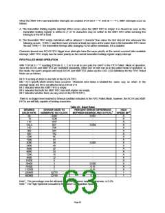
Table 30 shows the baud rates.
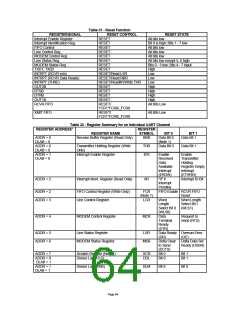
Effect Of The Reset on Register File
The Reset Function (Table 31) details the effect of the Reset input on each of the registers of the Serial Port.
FIFO INTERRUPT MODE OPERATION
When the RCVR FIFO and receiver interrupts are enabled (FCR bit 0 = "1", IER bit 0 = "1"), RCVR interrupts occur as
follows:
A. The receive data available interrupt will be issued when the FIFO has reached its programmed trigger level; it is
cleared as soon as the FIFO drops below its programmed trigger level.
B. The IIR receive data available indication also occurs when the FIFO trigger level is reached. It is cleared when the
FIFO drops below the trigger level.
C. The receiver line status interrupt (IIR=06H), has higher priority than the received data available (IIR=04H) interrupt.
D. The data ready bit (LSR bit 0) is set as soon as a character is transferred from the shift register to the RCVR FIFO. It
is reset when the FIFO is empty.
When RCVR FIFO and receiver interrupts are enabled, RCVR FIFO timeout interrupts occur as follows:
A. A FIFO timeout interrupt occurs if all the following conditions exist:
-
-
At least one character is in the FIFO.
The most recent serial character received was longer than 4 continuous character times ago. (If 2 stop bits are
programmed, the second one is included in this time delay).
-
The most recent CPU read of the FIFO was longer than 4 continuous character times ago.
This will cause a maximum character received to interrupt issued delay of 160 msec at 300 BAUD with a 12 bit
character.
B. Character times are calculated by using the RCLK input for a clock signal (this makes the delay proportional to the
baudrate).
C. When a timeout interrupt has occurred it is cleared and the timer reset when the CPU reads one character from the
RCVR FIFO.
D. When a timeout interrupt has not occurred the timeout timer is reset after a new character is received or after the
CPU reads the RCVR FIFO.
Page 62

 SMSC [ SMSC CORPORATION ]