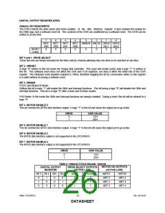
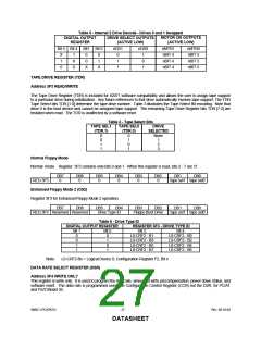
Table 5 - Internal 2 Drive Decode - Drives 0 and 1 Swapped
MOTOR ON OUTPUTS
(ACTIVE LOW)
DIGITAL OUTPUT
DRIVE SELECT OUTPUTS
REGISTER
(ACTIVE LOW)
Bit 5 Bit 4 Bit1 Bit 0
nDS1
nDS0
nMTR1
nMTR0
nBIT 5
nBIT 5
nBIT 5
X
1
0
1
X
0
0
0
X
0
1
X
0
1
1
1
0
1
nBIT 4
nBIT 4
nBIT 4
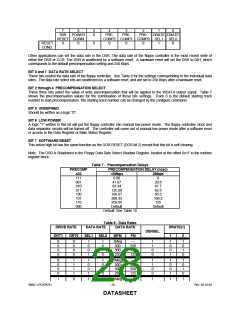
TAPE DRIVE REGISTER (TDR)
Address 3F3 READ/WRITE
The Tape Drive Register (TDR) is included for 82077 software compatibility and allows the user to assign tape support
to a particular drive during initialization. Any future references to that drive automatically invokes tape support. The TDR
Tape Select bits TDR.[1:0] determine the tape drive number. Table 3 illustrates the Tape Select Bit encoding. Note that
drive 0 is the boot device and cannot be assigned tape support. The remaining Tape Drive Register bits TDR.[7:2] are
tristated when read. The TDR is unaffected by a software reset.
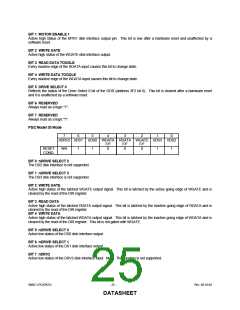
Table 3 - Tape Select Bits
TAPE SEL1
TAPE SEL0
DRIVE
(TDR.1)
(TDR.0)
SELECTED
0
0
1
1
0
1
0
1
None
1
2
3
Normal Floppy Mode
Normal mode. Register 3F3 contains only bits 0 and 1. When this register is read, bits 2 - 7 are ‘0’.
DB7
0
DB6
0
DB5
0
DB4
0
DB3
0
DB2
0
DB1
DB0
REG 3F3
tape sel1 tape sel0
Enhanced Floppy Mode 2 (OS2)
Register 3F3 for Enhanced Floppy Mode 2 operation.
DB7 DB6 DB5 DB4
DB3
DB2
DB1
DB0
REG 3F3 Reserved Reserved Drive Type ID
Floppy Boot Drive
tape sel1 tape sel0
Table 6 - Drive Type ID
DIGITAL OUTPUT REGISTER
REGISTER 3F3 - DRIVE TYPE ID
Bit 1
Bit 0
Bit 5
Bit 4
0
0
1
1
0
1
0
1
L0-CRF2 - B1
L0-CRF2 - B3
L0-CRF2 - B5
L0-CRF2 - B7
L0-CRF2 - B0
L0-CRF2 - B2
L0-CRF2 - B4
L0-CRF2 - B6
Note:
L0-CRF2-Bx = Logical Device 0, Configuration Register F2, Bit x.
DATA RATE SELECT REGISTER (DSR)
Address 3F4 WRITE ONLY
This register is write only. It is used to program the data rate, amount of write precompensation, power down status, and
software reset. The data rate is programmed using the Configuration Control Register (CCR) not the DSR, for PC/AT
and PS/2 Model 30.
SMSC LPC47B27x
- 27 -
Rev. 08-10-04
DATASHEET

 SMSC [ SMSC CORPORATION ]