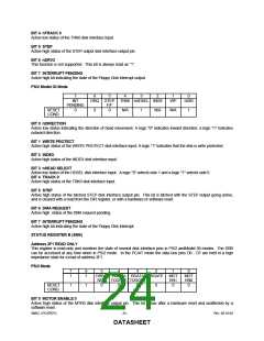
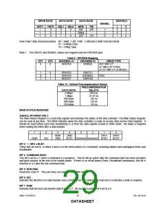
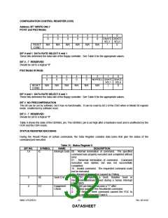
7
6
5
0
4
3
2
1
0
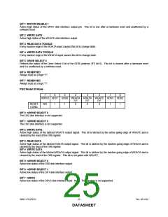
S/W
POWER
PRE-
PRE-
PRE-
DRATE DRATE
RESET DOWN
COMP2 COMP1 COMP0 SEL1
SEL0
0
RESET
COND.
0
0
0
0
0
0
1
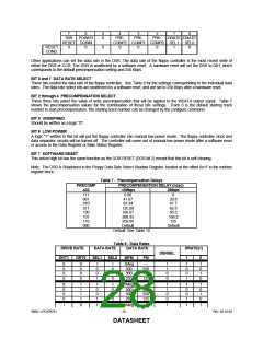
Other applications can set the data rate in the DSR. The data rate of the floppy controller is the most recent write of
either the DSR or CCR. The DSR is unaffected by a software reset. A hardware reset will set the DSR to 02H, which
corresponds to the default precompensation setting and 250 Kbps.
BIT 0 and 1 DATA RATE SELECT
These bits control the data rate of the floppy controller. See Table 8 for the settings corresponding to the individual data
rates. The data rate select bits are unaffected by a software reset, and are set to 250 Kbps after a hardware reset.
BIT 2 through 4 PRECOMPENSATION SELECT
These three bits select the value of write precompensation that will be applied to the WDATA output signal. Table 7
shows the precompensation values for the combination of these bits settings. Track 0 is the default starting track
number to start precompensation. this starting track number can be changed by the configure command.
BIT 5 UNDEFINED
Should be written as a logic "0".
BIT 6 LOW POWER
A logic "1" written to this bit will put the floppy controller into manual low power mode. The floppy controller clock and
data separator circuits will be turned off. The controller will come out of manual low power mode after a software reset
or access to the Data Register or Main Status Register.
BIT 7 SOFTWARE RESET
This active high bit has the same function as the DOR RESET (DOR bit 2) except that this bit is self clearing.
Note: The DSR is Shadowed in the Floppy Data Rate Select Shadow Register, located at the offset 0x1F in the runtime
register block.
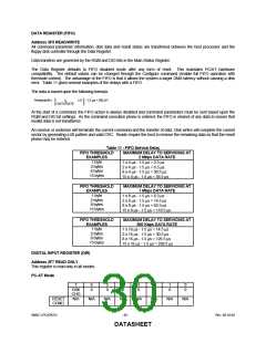
Table 7 - Precompensation Delays
PRECOMP
432
PRECOMPENSATION DELAY (nsec)
<2Mbps
0.00
2Mbps
0
111
001
41.67
20.8
41.7
62.5
83.3
104.2
125
010
83.34
011
125.00
100
166.67
101
208.33
110
250.00
000
Default
Default
Default: See Table 10
Table 8 - Data Rates
DRIVE RATE
DATA RATE
DATA RATE
DRATE(1)
DENSEL
DRT1
DRT0
SEL1
SEL0
MFM
FM
1
0
0
0
0
0
0
0
0
0
1
0
0
1
1
0
1
0
1Meg
500
---
1
1
0
0
1
0
0
1
1
0
1
0
250
150
125
300
250
0
0
0
0
1
1
1
1
1
0
0
1
1
0
1
0
1Meg
500
---
1
1
0
0
1
0
0
1
1
0
1
0
250
250
125
500
250
1
0
1
1
1Meg
---
1
1
1
SMSC LPC47B27x
- 28 -
Rev. 08-10-04
DATASHEET

 SMSC [ SMSC CORPORATION ]