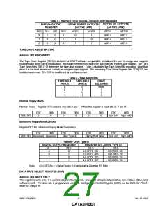
BIT 0 - 6 UNDEFINED
The data bus outputs D0 - 6 are read as ‘0’.
BIT 7 DSKCHG
This bit monitors the pin of the same name and reflects the opposite value seen on the disk cable or the value
programmed in the Force Disk Change Register (see Runtime Register at offset 0x1E).
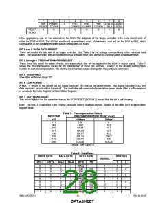
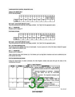
PS/2 Mode
7
6
1
5
1
4
1
3
1
2
1
0
DSK
CHG
N/A
DRATE DRATE nHIGH
SEL1
N/A
SEL0 nDENS
N/A
RESET
COND.
N/A
N/A
N/A
N/A
1
BIT 0 nHIGH DENS
This bit is low whenever the 500 Kbps or 1 Mbps data rates are selected, and high when 250 Kbps and 300 Kbps are
selected.
BITS 1 - 2 DATA RATE SELECT
These bits control the data rate of the floppy controller. See Table 8 for the settings corresponding to the individual data
rates. The data rate select bits are unaffected by a software reset, and are set to 250 Kbps after a hardware reset.
BITS 3 - 6 UNDEFINED
Always read as a logic "1"
BIT 7 DSKCHG
This bit monitors the pin of the same name and reflects the opposite value seen on the disk cable or the value
programmed in the Force Disk Change Register (see Runtime Register at offset 0x1E).
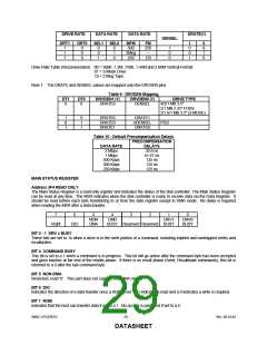
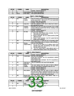
Model 30 Mode
7
6
0
5
0
4
0
3
2
1
0
DSK
CHG
N/A
DMAEN NOPREC DRATE DRATE
SEL1
1
SEL0
0
RESET
COND.
0
0
0
0
0
BITS 0 - 1 DATA RATE SELECT
These bits control the data rate of the floppy controller. See Table 8 for the settings corresponding to the individual data
rates. The data rate select bits are unaffected by a software reset, and are set to 250 Kbps after a hardware reset.
BIT 2 NOPREC
This bit reflects the value of NOPREC bit set in the CCR register.
BIT 3 DMAEN
This bit reflects the value of DMAEN bit set in the DOR register bit 3.
BITS 4 - 6 UNDEFINED
Always read as a logic "0"
BIT 7 DSKCHG
This bit monitors the pin of the same name and reflects the opposite value seen on the disk cable or the value
programmed in the Force Disk Change Register (see Runtime Register at offset 0x1E).
SMSC LPC47B27x
- 31 -
Rev. 08-10-04
DATASHEET

 SMSC [ SMSC CORPORATION ]