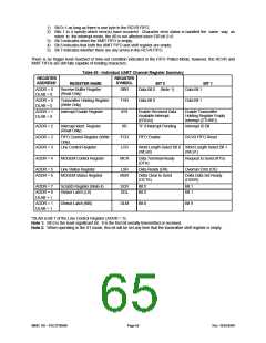
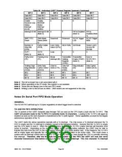
Table 56 - Individual UART Channel Register Summary Continued
BIT 2
Data Bit 2
Data Bit 2
Enable
BIT 3
Data Bit 3
Data Bit 3
Enable
BIT 4
Data Bit 4
Data Bit 4
0
BIT 5
Data Bit 5
Data Bit 5
0
BIT 6
Data Bit 6
Data Bit 6
0
BIT 7
Data Bit 7
Data Bit 7
0
Receiver Line MODEM
Status
Status
Interrupt
Interrupt
(ELSI)
(EMSI)
Interrupt ID Bit Interrupt ID Bit
(Note 5)
0
0
FIFOs Enabled FIFOs
(Note 5) Enabled (Note
5)
XMIT FIFO
Reset
DMA Mode
Select (Note
6)
Reserved
Reserved
RCVR Trigger RCVR Trigger
LSB
MSB
Number of
Stop Bits
(STB)
Parity Enable Even Parity
Stick Parity Set Break
Divisor Latch
Access Bit
(DLAB)
(PEN)
Select (EPS)
OUT1
(Note 3)
OUT2
(Note 3)
Loop
0
0
0
Parity Error
Framing Error Break
Transmitter Transmitter
Error in
(PE)
(FE)
Interrupt (BI) Holding
Empty (TEMT) RCVR FIFO
Register
(Note 2)
(Note 5)
(THRE)
Trailing Edge Delta Data
Clear to
Data Set
Ring Indicator
(RI)
Data Carrier
Ring Indicator Carrier Detect Send (CTS) Ready
Detect (DCD)
(TERI)
Bit 2
(DDCD)
Bit 3
(DSR)
Bit 5
Bit 5
Bit 4
Bit 4
Bit 12
Bit 6
Bit 6
Bit 14
Bit 7
Bit 7
Bit 15
Bit 2
Bit 3
Bit 10
Bit 11
Bit 13
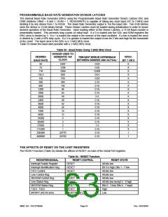
Note 3: This bit no longer has a pin associated with it.
Note 4: When operating in the XT mode, this register is not available.
Note 5: These bits are always zero in the non-FIFO mode.
Note 6: Writing a one to this bit has no effect. DMA modes are not supported in this chip.
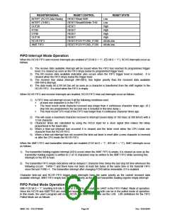
Notes On Serial Port FIFO Mode Operation
GENERAL
The RCVR FIFO will hold up to 16 bytes regardless of which trigger level is selected.
TX AND RX FIFO OPERATION
The Tx portion of the UART transmits data through TXD as soon as the CPU loads a byte into the Tx FIFO. The
UART will prevent loads to the Tx FIFO if it currently holds 16 characters. Loading to the Tx FIFO will again be
enabled as soon as the next character is transferred to the Tx shift register. These capabilities account for the largely
autonomous operation of the Tx.
The UART starts the above operations typically with a Tx interrupt. The chip issues a Tx interrupt whenever the Tx
FIFO is empty and the Tx interrupt is enabled, except in the following instance. Assume that the Tx FIFO is empty
and the CPU starts to load it. When the first byte enters the FIFO the Tx FIFO empty interrupt will transition from
active to inactive. Depending on the execution speed of the service routine software, the UART may be able to
transfer this byte from the FIFO to the shift register before the CPU loads another byte. If this happens, the Tx FIFO
will be empty again and typically the UART’s interrupt line would transition to the active state. This could cause a
system with an interrupt control unit to record a Tx FIFO empty condition, even though the CPU is currently servicing
that interrupt. Therefore, after the first byte has been loaded into the FIFO the UART will wait one serial
character transmission time before issuing a new Tx FIFO empty interrupt. This one character Tx interrupt
SMSC DS – FDC37N3869
Page 66
Rev. 10/25/2000

 SMSC [ SMSC CORPORATION ]