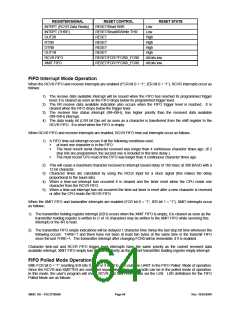
1) Bit 0=1 as long as there is one byte in the RCVR FIFO.
2) Bits 1 to 4 specify which error(s) have occurred. Character error status is handled the same way as
when in the interrupt mode, the IIR is not affected since EIR bit 2=0.
3) Bit 5 indicates when the XMIT FIFO is empty.
4) Bit 6 indicates that both the XMIT FIFO and shift register are empty.
5) Bit 7 indicates whether there are any errors in the RCVR FIFO.
There is no trigger level reached or time-out condition indicated in the FIFO Polled Mode, however, the RCVR and
XMIT FIFOs are still fully capable of holding characters.
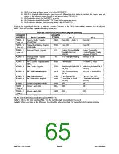
Table 55 - Individual UART Channel Register Summary
REGISTER
ADDRESS*
REGISTER
SYMBOL
REGISTER NAME
BIT 0
BIT 1
ADDR = 0
DLAB = 0
ADDR = 0
DLAB = 0
ADDR = 1
DLAB = 0
Receive Buffer Register
RBR
THR
IER
Data Bit 0 (Note 1)
Data Bit 1
Data Bit 1
(Read Only)
Transmitter Holding Register
(Write Only)
Interrupt Enable Register
Data Bit 0
Enable Received Data
Available Interrupt
(ERDAI)
Enable Transmitter
Holding Register Empty
Interrupt (ETHREI)
ADDR = 2
Interrupt Ident. Register
(Read Only)
IIR
”0” if Interrupt Pending
Interrupt ID Bit
ADDR = 2
ADDR = 3
FIFO Control Register (Write
FCR
LCR
FIFO Enable
RCVR FIFO Reset
Only)
Line Control Register
Word Length Select Bit 0 Word Length Select Bit 1
(WLS0)
(WLS1)
ADDR = 4
MODEM Control Register
MCR
Data Terminal Ready
(DTR)
Request to Send (RTS)
ADDR = 5
ADDR = 6
Line Status Register
MODEM Status Register
LSR
MSR
Data Ready (DR)
Overrun Error (OE)
Delta Clear to Send
Delta Data Set Ready
(DCTS)
(DDSR)
ADDR = 7
ADDR = 0
DLAB = 1
ADDR = 1
DLAB = 1
Scratch Register (Note 4)
Divisor Latch (LS)
SCR
DDL
Bit 0
Bit 0
Bit 1
Bit 1
Divisor Latch (MS)
DLM
Bit 8
Bit 9
*DLAB is Bit 7 of the Line Control Register (ADDR = 3).
Note 1: Bit 0 is the least significant bit. It is the first bit serially transmitted or received.
Note 2: When operating in the XT mode, this bit will be set any time that the transmitter shift register is empty.
SMSC DS – FDC37N3869
Page 65
Rev. 10/25/2000

 SMSC [ SMSC CORPORATION ]