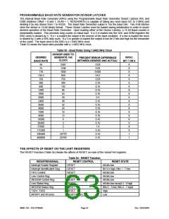
delay will remain active until at least two bytes have been loaded into the FIFO, concurrently. When the Tx
FIFO empties after this condition, the Tx interrupt will be activated without a one character delay.
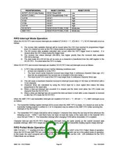
Rx support functions and operation are quite different from those described for the transmitter. The Rx FIFO receives
data until the number of bytes in the FIFO equals the selected interrupt trigger level. At that time if Rx interrupts are
enabled, the UART will issue an interrupt to the CPU. The Rx FIFO will continue to store bytes until it holds 16 of
them. It will not accept any more data when it is full. Any more data entering the Rx shift register will set the Overrun
Error flag. Normally, the FIFO depth and the programmable trigger levels will give the CPU ample time to empty the
Rx FIFO before an overrun occurs.
One side-effect of having a Rx FIFO is that the selected interrupt trigger level may be above the data level in the
FIFO. This could occur when data at the end of the block contains fewer bytes than the trigger level. No interrupt
would be issued to the CPU and the data would remain in the UART. To prevent the software from having to
check for this situation the chip incorporates a time-out interrupt.
The time-out interrupt is activated when there is a least one byte in the Rx FIFO, and neither the CPU nor the Rx shift
register has accessed the Rx FIFO within 4 character times of the last byte. The time-out interrupt is cleared or reset
when the CPU reads the Rx FIFO or another character enters it.
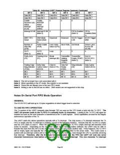
These FIFO related features allow optimization of CPU/UART transactions and are especially useful given the higher
baud rate capability (256K baud).
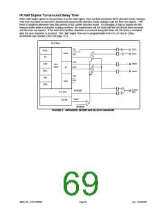
INFRARED INTERFACE
The FDC37N3869 infrared interface provides a two-way wireless communications port using infrared as the
transmission medium. Several infrared protocols have been provided in this implementation including IrDA v1.1
(SIR/FIR), ASKIR, and Consumer IR (Figure 3). For more information consult the SMSC Infrared Communication
Controller (IRCC) specification.
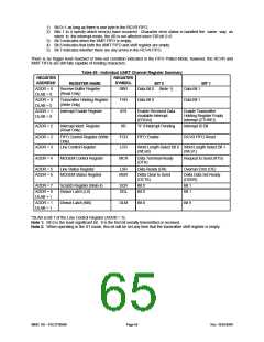
The IrDA v1.0 (SIR) and ASKIR formats are driven by the ACE registers found in UART2. The UART2 registers are
described in section
SERIAL PORT (UART) starting on page 56. The base address for UART2 is programmed in CR25, the UART2 Base
Address Register (see section CR25 on page 110).
The IrDA V1.2 (FIR) and Consumer IR formats are driven by the SCE registers. Descriptions of these registers can
be found in the SMSC Infrared Communications Controller Specification. The Base Address for the SCE registers is
programmed in CR2B, the SCE Base Address Register (see section CR28 on page 111).
IrDA SIR/FIR and ASKIR
IrDA SIR (v1.0) specifies asynchronous serial communication at baud rates up to 115.2Kbps. Each byte is sent
serially LSB first beginning with a zero value start bit. A zero is signaled by sending a single infrared pulse at the
beginning of the serial bit time. A one is signaled by the absence of an infrared pulse during the bit time. Please refer
to section AC TIMING for the parameters of these pulses and the IrDA waveforms.
IrDA FIR (v1.2) includes IrDA v1.0 SIR and additionally specifies synchronous serial communications at data rates up
to 4Mbps.
Data is transferred LSB first in packets that can be up to 2048 bits in length. IrDA v1.2 includes .576Mbps and
1.152Mbps data rates using an encoding scheme that is similar to SIR. The 4Mbps data rate uses a pulse position
modulation (PPM) technique.
The ASKIR infrared allows asynchronous serial communication at baud rates up to 19.2Kbps. Each byte is sent
serially LSB first beginning with a zero value start bit. A zero is signaled by sending a 500KHz carrier waveform for
the duration of the serial bit time. A one is signaled by the absence of carrier during the bit time. Please refer to
section AC TIMING for the parameters of the ASKIR waveforms.
Consumer IR
The FDC37N3869 Consumer IR interface is a general-purpose Amplitude Shift Keyed encoder/decoder with
programmable carrier and bit-cell rates that can emulate many popular TV Remote encoding formats; including,
38KHz PPM, PWM and RC-5. The carrier frequency is programmable from 1.6MHz to 6.25KHz. The bit-cell rate
range is 100KHz to 390Hz.
SMSC DS – FDC37N3869
Page 67
Rev. 10/25/2000

 SMSC [ SMSC CORPORATION ]