PROGRAMMABLE BAUD RATE GENERATOR DIVISOR LATCHES
The internal Baud Rate Generator (BRG) using the Programmable Baud Rate Generator Divisor Latches DDL and
DDM (Address Offset = 0 and 1, DLAB = 1, READ/WRITE) is capable of taking any clock input (DC to 3 MHz) and
dividing it by any divisor from 1 to 65535. The Baud Rate Generator output is 16x the baud rate. Two 8-bit latches
store the divisor in 16-bit binary format. These Divisor Latches must be loaded during initialization in order to insure
desired operation of the Baud Rate Generator. Upon loading either of the Divisor Latches, a 16 bit Baud counter is
immediately loaded. This prevents long counts on initial load. If a 0 is loaded into the DDL and DDM registers the
BRG clock is divided by 3. If a 1 is loaded the output is the inverse of the input oscillator. If a two is loaded the clock
is divided by 2 with a 50% duty cycle. If a 3 or greater is loaded the output is low for 2 bits and high for the remainder
of the count. The input clock to the BRG is a 1.8462 MHz clock.
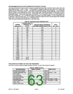
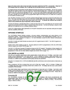
Table 53 shows the baud rates possible with a 1.8462 MHz clock.
Table 53 - Baud Rates Using 1.8462 MHz Clock
DIVISOR USED TO
DESIRED
BAUD RATE
50
GENERATE 16X
CLOCK
CROC:
PERCENT ERROR DIFFERENCE
BETWEEN DESIRED AND ACTUAL*
BIT 7 OR 6
2307
1538
1049
858
769
384
192
96
0.03
0.03
0.005
0.01
0.03
0.16
0.16
0.16
0.16
0.5
X
X
X
X
X
X
X
X
X
X
X
X
X
X
X
X
X
X
X
1
75
110
134.5
150
300
600
1200
1800
2000
2400
3600
4800
7200
64
58
48
32
24
16
12
6
3
2
0.16
0.16
0.16
0.16
0.16
0.16
0.16
1.6
9600
19200
38400
57600
115200
230400
460800
1
0.16
0.16
0.16
32770
32769
1
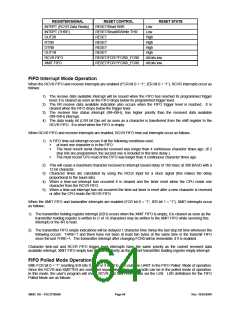
THE AFFECTS OF RESET ON THE UART REGISTERS
The RESET Function (Table 54) details the affects of RESET on each of the Serial Port registers.
Table 54 - RESET Function
REGISTER/SIGNAL
Interrupt Enable Register
Interrupt Identification Reg.
FIFO Control
RESET CONTROL
RESET STATE
All bits low
Bit 0 is high; Bits 1 - 7 low
All bits low
RESET
RESET
RESET
Line Control Reg.
RESET
All bits low
MODEM Control Reg.
Line Status Reg.
MODEM Status Reg.
TXD1, TXD2
RESET
RESET
RESET
RESET
All bits low
All bits low except 5 - 6 high
Bits 0 - 3 low; Bits 4 - 7 input
High
INTRPT (RCVR errs)
RESET/Read LSR
Low
SMSC DS – FDC37N3869
Page 63
Rev. 10/25/2000

 SMSC [ SMSC CORPORATION ]