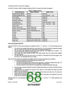
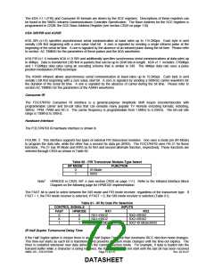
The Affects of RESET on the UART Registers
The RESET Function (Table 57) details the affects of RESET on each of the Serial Port registers.
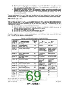
Table 57 - RESET Function
REGISTER/SIGNAL
Interrupt Enable Register
Interrupt Identification Reg.
FIFO Control
RESET CONTROL
RESET
RESET STATE
All bits low
RESET
Bit 0 is high; Bits 1 - 7 low
RESET
All bits low
Line Control Reg.
MODEM Control Reg.
Line Status Reg.
MODEM Status Reg.
TXD1, TXD2
RESET
All bits low
RESET
All bits low
RESET
All bits low except 5 - 6 high
RESET
Bits 0 - 3 low; Bits 4 - 7 input
RESET
High
INTRPT (RCVR errs)
INTRPT (RCVR Data Ready)
INTRPT (THRE)
OUT2B
RESET/Read LSR
RESET/Read RBR
RESET/ReadIIR/Write THR
RESET
Low
Low
Low
High
RTSB
RESET
High
DTRB
RESET
High
OUT1B
RESET
High
RCVR FIFO
RESET/FCR1*FCR0/_FCR0
RESET/FCR1*FCR0/_FCR0
All bits low
All bits low
XMIT FIFO
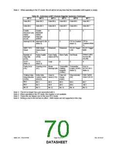
FIFO Interrupt Mode Operation
When the RCVR FIFO and receiver interrupts are enabled (FCR bit 0 = “1”, IER bit 0 = “1”), RCVR interrupts occur as
follows:
1. The receive data available interrupt will be issued when the FIFO has reached its programmed trigger
level; it is cleared as soon as the FIFO drops below its programmed trigger level.
2. The IIR receive data available indication also occurs when the FIFO trigger level is reached. It is
cleared when the FIFO drops below the trigger level.
3. The receiver line status interrupt (IIR=06H), has higher priority than the received data available
(IIR=04H) interrupt.
4. The data ready bit (LSR bit 0)is set as soon as a character is transferred from the shift register to the
RCVR FIFO. It is reset when the FIFO is empty.
When RCVR FIFO and receiver interrupts are enabled, RCVR FIFO time-out interrupts occur as follows:
1. A FIFO time-out interrupt occurs if all the following conditions exist:
at least one character is in the FIFO
The most recent serial character received was longer than 4 continuous character times ago. (If 2
stop bits are programmed, the second one is included in this time delay.)
The most recent CPU read of the FIFO was longer than 4 continuous character times ago.
2. This will cause a maximum character received to interrupt issued delay of 160 msec at 300 BAUD with a
12 bit character.
3. Character times are calculated by using the RCLK input for a clock signal (this makes the delay
proportional to the baud rate).
4. When a time-out interrupt has occurred it is cleared and the timer reset when the CPU reads one
character from the RCVR FIFO.
5. When a time-out interrupt has not occurred the time-out timer is reset after a new character is received
or after the CPU reads the RCVR FIFO.
When the XMIT FIFO and transmitter interrupts are enabled (FCR bit 0 = “1”, IER bit 1 = “1”), XMIT interrupts occur
as follows:
SMSC DS – FDC37N769
Page 68 of 137
Rev. 02-16-07
DATASHEET

 SMSC [ SMSC CORPORATION ]