1. The transmitter holding register interrupt (02H) occurs when the XMIT FIFO is empty; it is cleared as
soon as the transmitter holding register is written to (1 of 16 characters may be written to the XMIT FIFO
while servicing this interrupt) or the IIR is read.
2. The transmitter FIFO empty indications will be delayed 1 character time minus the last stop bit time
whenever the following occurs: THRE=1 and there have not been at least two bytes at the same time in
the transmit FIFO since the last THRE=1. The transmitter interrupt after changing FCR0 will be
immediate, if it is enabled.
Character time-out and RCVR FIFO trigger level interrupts have the same priority as the current received data
available interrupt; XMIT FIFO empty has the same priority as the current transmitter holding register empty interrupt.
FIFO Polled Mode Operation
With FCR bit 0 = “1” resetting IER bits 0, 1, 2 or 3 or all to zero puts the UART in the FIFO Polled Mode of operation.
Since the RCVR and XMITTER are controlled separately, either one or both can be in the polled mode of operation.
In this mode, the user’s program will check RCVR and XMITTER status via the LSR. LSR definitions for the FIFO
Polled Mode are as follows:
1. Bit 0=1 as long as there is one byte in the RCVR FIFO.
2. Bits 1 to 4 specify which error(s) have occurred. Character error status is handled the same way as
when in the interrupt mode, the IIR is not affected since EIR bit 2=0.
3. Bit 5 indicates when the XMIT FIFO is empty.
4. Bit 6 indicates that both the XMIT FIFO and shift register are empty.
5. Bit 7 indicates whether there are any errors in the RCVR FIFO.
There is no trigger level reached or time-out condition indicated in the FIFO Polled Mode, however, the RCVR and
XMIT FIFOs are still fully capable of holding characters.
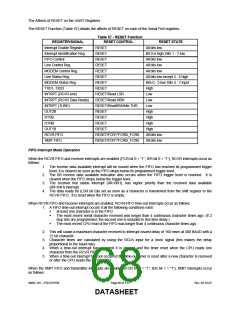
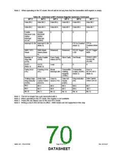
Table 58 - Individual UART Channel Register Summary
REGISTER
ADDRESS*
REGISTER
SYMBOL
REGISTER NAME
BIT 0
BIT 1
ADDR = 0
DLAB = 0
Receive Buffer Register
(Read Only)
RBR
THR
IER
Data Bit 0 (Note Data Bit 1
1)
ADDR = 0
DLAB = 0
Transmitter Holding
Register (Write Only)
Data Bit 0
Data Bit 1
ADDR = 1
DLAB = 0
Interrupt Enable Register
Enable Received
Data Available
Interrupt (ERDAI)
Enable Transmitter
Holding Register
Empty Interrupt
(ETHREI)
ADDR = 2
ADDR = 2
ADDR = 3
Interrupt Ident. Register
(Read Only)
IIR
”0” if Interrupt
Pending
Interrupt ID Bit
FIFO Control Register
(Write Only)
FCR
LCR
FIFO Enable
RCVR FIFO Reset
Word Length
Select Bit 0
(WLS0)
Line Control Register
Word Length
Select Bit 1
(WLS1)
ADDR = 4
MODEM Control Register
MCR
Data Terminal
Ready (DTR)
Request to Send
(RTS)
ADDR = 5
ADDR = 6
Data Ready (DR)
Line Status Register
LSR
Overrun Error (OE)
Delta Clear to
Send (DCTS)
MODEM Status Register
MSR
Delta Data Set
Ready (DDSR)
ADDR = 7
Scratch Register (Note 4)
Divisor Latch (LS)
SCR
DDL
Bit 0
Bit 0
Bit 1
Bit 1
ADDR = 0
DLAB = 1
ADDR = 1
DLAB = 1
Divisor Latch (MS)
DLM
Bit 8
Bit 9
*DLAB is Bit 7 of the Line Control Register (ADDR = 3).
Note 1: Bit 0 is the least significant bit. It is the first bit serially transmitted or received.
SMSC DS – FDC37N769
Page 69 of 137
Rev. 02-16-07
DATASHEET

 SMSC [ SMSC CORPORATION ]