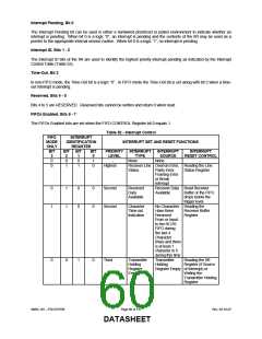
OUT1, Bit 2
The OUT1 bit controls the Output 1 (OUT1) bit. This bit does not have an output pin and can only be read or written
by the CPU.
OUT2, Bit 3
The OUT2 bit is used to enable the UART interrupt. When OUT2 is a logic “0”, the serial port interrupt output is
forced to a high impedance state; i.e, disabled. When OUT2 is a logic “1”, the serial port interrupt outputs are
enabled.
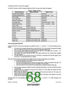
Loop, Bit 4
The Loop bit provides the loopback feature for diagnostic testing of the Serial Port. When bit 4 is set to logic “1”, the
following occurs:
1. The TXD is set to the Marking State (logic “1”).
2. The receiver Serial Input (RXD) is disconnected.
3. The output of the Transmitter Shift Register is “looped back” into the Receiver Shift Register input.
4. All MODEM Control inputs (nCTS, nDSR, nRI and nDCD) are disconnected.
5. The four MODEM Control outputs (nDTR, nRTS, OUT1 and OUT2) are internally connected to the four
MODEM Control inputs (nDSR, nCTS, RI and DCD) respectively.
6. The Modem Control output pins are forced inactive.
7. Data that is transmitted is immediately received.
The Loopback feature allows the processor to verify the transmit and receive data paths of the Serial Port. The
receiver and the transmitter interrupts are fully operational in loopback mode. The MODEM Control Interrupts are
also operational but the interrupts’ sources are now the lower four bits of the MODEM Control Register instead of the
MODEM Control inputs. The interrupts are still controlled by the Interrupt Enable Register.
Reserved, Bits 5 - 7
Bits 5 to 7 are RESERVED. Reserved bits cannot be written and return 0 when read.
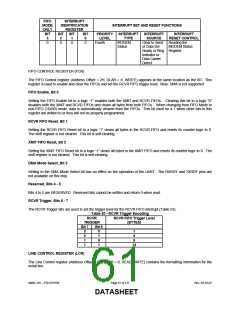
LINE STATUS REGISTER (LSR)
Address Offset = 5H, DLAB = X, READ/WRITE
Data Ready, Bit 0
Data Ready (DR) is set to a logic “1” whenever a complete received data character has been transferred into the
Receiver Buffer Register or the FIFO. DR is reset to a logic “0” by reading all of the data in the Receive Buffer
Register or the FIFO.
Overrun Error, Bit 1
The Overrun Error (OE) bit indicates that data in the Receiver Buffer Register was not read before the next character
was transferred into the register, thereby destroying the previous character. In FIFO mode, an overrun error will occur
only when the FIFO is full and the next character has been completely received in the shift register: the character in
the shift register is overwritten but not transferred to the FIFO. The OE indicator is set to a logic “1” immediately upon
detection of an overrun condition and reset whenever the Line Status Register is read.
Parity Error, Bit 2
The Parity Error (PE) bit indicates that the received data character does not have the correct even or odd parity, as
selected by the even parity select bit. The PE is set to a logic “1” upon detection of a parity error and is reset to a
logic “0” whenever the Line Status Register is read. In the FIFO mode this error is associated with the particular
character in the FIFO it applies to. This error is indicated when the associated character is at the top of the FIFO.
Framing Error, Bit 3
The Framing Error (FE) bit indicates that the received character did not have a valid stop bit. Bit 3 is set to a logic “1”
whenever the stop bit following the last data bit or parity bit is detected as a zero bit (Spacing level). The FE is reset
to a logic “0” whenever the Line Status Register is read. In the FIFO mode this error is associated with the particular
SMSC DS – FDC37N769
Page 64 of 137
Rev. 02-16-07
DATASHEET

 SMSC [ SMSC CORPORATION ]