Clear To Send, Bit 4
The Clear To Send bit is the complement of the Clear To Send input (nCTS). If the Loop bit of the MCR is set to logic
“1”, this bit is equivalent to nRTS in the MCR.
Data Set Ready, Bit 5
The Data Set Ready bit is the complement of the Data Set Ready input (nDSR). If the Loop bit of the MCR is set to
logic “1”, this bit is equivalent to DTR in the MCR.
Ring Indicator, Bit 6
The Ring Indicator bit is the complement of the Ring Indicator input (nRI). If the Loop bit of the MCR is set to logic
“1”, this bit is equivalent to OUT1 in the MCR.
Data Carrier Detect, Bit 7
The Data Carrier Detect bit is the complement of the Data Carrier Detect input (nDCD). If the Loop bit of the MCR is
set to logic “1”, this bit is equivalent to OUT2 in the MCR.
SCRATCHPAD REGISTER (SCR)
The Scratchpad register (Address Offset =7H, DLAB =X, READ/WRITE) has no effect on the operation of the Serial
Port. It is intended as a scratchpad register to be used by the programmer to hold data temporarily.
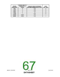
PROGRAMMABLE BAUD RATE GENERATOR DIVISOR LATCHES
The internal Baud Rate Generator (BRG) using the Programmable Baud Rate Generator Divisor Latches DDL and
DDM (Address Offset = 0 and 1, DLAB = 1, READ/WRITE) is capable of taking any clock input (DC to 3 MHz) and
dividing it by any divisor from 1 to 65535. The Baud Rate Generator output is 16x the baud rate. Two 8-bit latches
store the divisor in 16-bit binary format. These Divisor Latches must be loaded during initialization in order to insure
desired operation of the Baud Rate Generator. Upon loading either of the Divisor Latches, a 16 bit Baud counter is
immediately loaded. This prevents long counts on initial load. If a 0 is loaded into the DDL and DDM registers the
BRG clock is divided by 3. If a 1 is loaded the output is the inverse of the input oscillator. If a two is loaded the clock
is divided by 2 with a 50% duty cycle. If a 3 or greater is loaded the output is low for 2 bits and high for the remainder
of the count. The input clock to the BRG is a 1.8462 MHz clock.
Table 56 shows the baud rates possible with a 1.8462 MHz clock.
Table 56 - Baud Rates Using 1.8462 MHz Clock
DIVISOR USED TO
DESIRED
BAUD RATE
50
GENERATE 16X
CLOCK
PERCENT ERROR DIFFERENCE
BETWEEN DESIRED AND ACTUAL*
0.03
CROC:
BIT 7 OR 6
X
2307
75
1538
1049
858
769
384
192
96
0.03
0.005
0.01
0.03
0.16
0.16
0.16
0.16
0.5
X
X
X
X
X
X
X
X
X
X
X
X
X
110
134.5
150
300
600
1200
1800
2000
2400
3600
4800
7200
64
58
48
0.16
0.16
0.16
0.16
32
24
16
SMSC DS – FDC37N769
Page 66 of 137
Rev. 02-16-07
DATASHEET

 SMSC [ SMSC CORPORATION ]