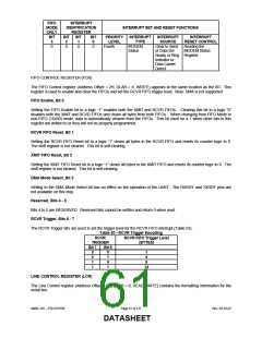
character in the FIFO it applies to. This error is indicated when the associated character is at the top of the FIFO.
The Serial Port will try to resynchronize after a framing error. To do this, it assumes that the framing error was due to
the next start bit, so it samples this ‘start’ bit twice and then takes in the ‘data’.
Break Interrupt, Bit 4
The Break Interrupt (BI) bit is set to a logic “1” whenever the received data input is held in the Spacing state (logic
“0”) for longer than a full word transmission time (that is, the total time of the start bit + data bits + parity bits + stop
bits). The BI is reset after the CPU reads the contents of the Line Status Register. In the FIFO mode this error is
associated with the particular character in the FIFO it applies to. This error is indicated when the associated character
is at the top of the FIFO. When break occurs only one zero character is loaded into the FIFO. Restarting after a
break is received requires the serial data (RXD) to be logic “1” for at least ½ bit time.
Note: LSR Bits 1 through 4 produce a Receiver Line Status Interrupt whenever any of the corresponding conditions
are detected and the interrupt is enabled.
Transmitter Holding Register Empty, Bit 5
The Transmitter Holding Register Empty (THRE) bit indicates that the Serial Port is ready to accept a new character
for transmission. In addition, this bit causes the Serial Port to issue an interrupt when the Transmitter Holding
Register interrupt enable is set high. The THRE bit is set to a logic “1” when a character is transferred from the
Transmitter Holding Register into the Transmitter Shift Register. The bit is reset to logic “0” whenever the CPU loads
the Transmitter Holding Register. In the FIFO mode this bit is set when the XMIT FIFO is empty, it is cleared when at
least 1 byte is written to the XMIT FIFO. Bit 5 is read-only.
Tranmitter Empty, Bit 6
The Transmitter Empty (TEMT) bit is set to a logic “1” whenever the Transmitter Holding Register (THR) and
Transmitter Shift Register (TSR) are both empty. It is reset to logic “0” whenever either the THR or TSR contains a
data character. Bit 6 is read-only. In the FIFO mode this bit is set whenever the THR and TSR are both empty.
RCVR FIFO Error, Bit 7
The RCVR FIFO Error bit is permanently set to logic “0” in the 450 mode. In the FIFO mode this bit is set to a logic
“1” when there is at least one parity error, framing error or break indication in the FIFO. This bit is cleared when the
LSR is read if there are no subsequent errors in the FIFO.
MODEM STATUS REGISTER (MSR)
The Modem Status register (Address Offset = 6H, DLAB = X, READ/WRITE) provides the current state of the control
lines from the MODEM or peripheral device. In addition to this current state information, four bits of the MODEM
Status Register provide state change information. These four bits are set to logic “1” whenever a control input
from the MODEM changes state. They are reset to logic “0” whenever the MODEM Status Register is read.
Delta Clear To Send, Bit 0
The Delta Clear To Send (DCTS) bit indicates that the nCTS input to the chip has changed state since the last
time the MSR was read.
Delta Data Set Ready, Bit 1
The Delta Data Set Ready (DDSR) bit indicates that the nDSR input has changed state since the last time the MSR
was read.
Trailing Edge Of Ring Indicator, Bit 2
The Trailing Edge of Ring Indicator (TERI) bit indicates that the nRI input has changed from logic “0” to logic “1”.
Delta Data Carrier Detect, Bit 3
The Delta Data Carrier Detect (DDCD) bit indicates that the nDCD input to the chip has changed state.
Note: Whenever bits 0, 1, 2, or 3 are set to a logic “1”, a MODEM Status Interrupt is generated.
SMSC DS – FDC37N769
Page 65 of 137
Rev. 02-16-07
DATASHEET

 SMSC [ SMSC CORPORATION ]