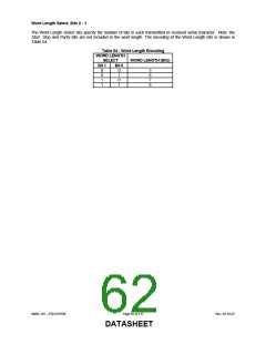
Stop Bits, Bit 2
The Stop Bits bit specifies the number of stop bits in each transmitted or received serial character. Table 55 describes
the Stop Bits encoding.
Table 55 - STOP Bit Encoding
STOP BITS
WORD
LENGTH
-
5 Bits
6 Bits
7 Bits
8 Bits
NUMBER OF
STOP BITS
(Bit 2)
0
0
1
1
1
1
1.5
2
2
2
Note:
The receiver ignores stop bits beyond the first, regardless of the number of stop bits used in transmitting.
Parity Enable, Bit 3
When the Parity Enable bit is a logic “1” a parity bit is generated (transmit data) or checked (receive data) between
the last data word bit and the first stop bit of the serial data. The parity bit is used to generate an even or odd number
of 1s when the data word bits and the parity bit are summed.
Even Parity Select, Bit 4
When the Even Parity Select (EPS) bit is a logic “0” and the Parity Enable is a logic “1”, an odd number of logic “1”’s
is transmitted or checked in the data word and the parity bit. When the Parity Enable is a logic “1” and the EPS bit is
a logic “1” an even number of bits is transmitted and checked.
Stick Parity, Bit 5
When the Stick Parity bit is a logic “1” and the Parity Enable is a logic “1”, the parity bit is transmitted and then
detected by the receiver in the opposite state indicated by the EPS bit.
Set Break, Bit 6
When the Set Break Control bit is a logic “1”, the transmit data output (TXD) is forced to the Spacing or logic “0” state
and remains there until reset by a low level bit 6, regardless of other transmitter activity. This feature enables the
Serial Port to alert a terminal in a communications system.
DLAB, Bit 7
The Divisor Latch Access Bit must be set high (logic “1”) to access the Divisor Latches of the Baud Rate Generator
during read or write operations. It must be set low (logic “0”) to access the Receiver Buffer Register, the Transmitter
Holding Register, or the Interrupt Enable Register.
MODEM CONTROL REGISTER (MCR)
The Modem Control register (Address Offset = 4H, DLAB = X, READ/WRITE) manages the interface for the MODEM,
data set, or device emulating a MODEM.
Data Terminal Ready, Bit 0
The Data Terminal Ready bit controls the Data Terminal Ready (nDTR) output. When bit 0 is set to a logic “1”,
the nDTR output is forced to a logic “0”. When bit 0 is a logic “0”, the nDTR output is forced to a logic “1”.
Request To Send, Bit 1
The Request To Send bit controls the Request To Send (nRTS) output. . When bit 1 is set to a logic “1”, the
nRTS output is forced to a logic “0”. When bit 1 is a logic “0”, the nRTS output is forced to a logic “1”.
SMSC DS – FDC37N769
Page 63 of 137
Rev. 02-16-07
DATASHEET

 SMSC [ SMSC CORPORATION ]