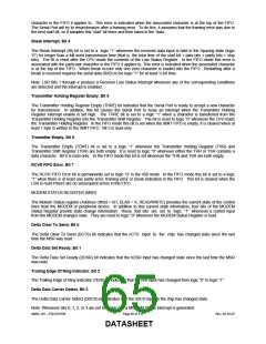
FIFO
MODE
ONLY
BIT
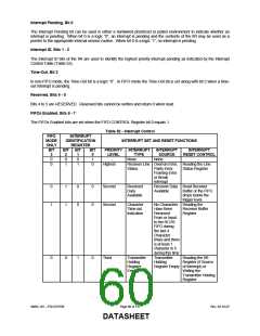
INTERRUPT
IDENTIFICATION
REGISTER
INTERRUPT SET AND RESET FUNCTIONS
BIT
2
BIT
1
BIT
0
PRIORITY
LEVEL
INTERRUPT
TYPE
MODEM
Status
INTERRUPT
SOURCE
Clear to Send
or Data Set
INTERRUPT
RESET CONTROL
Reading the
3
0
0
0
0
Fourth
MODEM Status
Ready or Ring Register
Indicator or
Data Carrier
Detect
FIFO CONTROL REGISTER (FCR)
The FIFO Control register (Address Offset = 2H, DLAB = X, WRITE) appears at the same location as the IIR. This
register is used to enable and clear the FIFOs and set the RCVR FIFO trigger level. Note: DMA is not supported.
FIFO Enable, Bit 0
Setting the FIFO Enable bit to a logic “1” enables both the XMIT and RCVR FIFOs. Clearing this bit to a logic “0”
disables both the XMIT and RCVR FIFOs and clears all bytes from both FIFOs. When changing from FIFO Mode to
non-FIFO (16450) mode, data is automatically cleared from the FIFOs. This bit must be a 1 when other bits in this
register are written to or they will not be properly programmed.
RCVR FIFO Reset, Bit 1
Setting the RCVR FIFO Reset bit to a logic “1” clears all bytes in the RCVR FIFO and resets its counter logic to 0.
The shift register is not cleared. This bit is self-clearing.
XMIT FIFO Reset, Bit 2
Setting the XMIT FIFO Reset bit to a logic “1” clears all bytes in the XMIT FIFO and resets its counter logic to 0. The
shift register is not cleared. This bit is self-clearing.
DMA Mode Select, Bit 3
Writing to the DMA Mode Select bit has no effect on the operation of the UART. The RXRDY and TXRDY pins are
not available on this chip.
Reserved, Bits 4 - 5
Bits 4 to 5 are RESERVED. Reserved bits cannot be written and return 0 when read.
RCVR Trigger, Bits 6 - 7
The RCVR Trigger bits are used to set the trigger level for the RCVR FIFO interrupt (Table 53).
Table 53 - RCVR Trigger Encoding
RCVR
TRIGGER
RCVR FIFO Trigger Level
(BYTES)
Bit 7
Bit 6
0
0
1
4
8
0
1
1
1
0
1
14
LINE CONTROL REGISTER (LCR)
The Line Control register (Address Offset = 3H, DLAB = 0, READ/WRITE) contains the formatting information for the
serial line.
SMSC DS – FDC37N769
Page 61 of 137
Rev. 02-16-07
DATASHEET

 SMSC [ SMSC CORPORATION ]