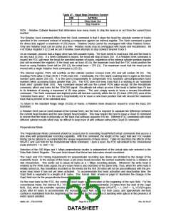
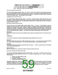
DLAB1
A2
0
0
A1
0
0
A0
0
1
REGISTER NAME
Divisor LSB (read/write)
Divisor MSB (read/write)
1
1
NOTE1: DLAB is Bit 7 of the Line Control Register
RECEIVE BUFFER REGISTER (RB)
The Receive Buffer register (Address Offset = 0H, DLAB = 0, READ ONLY) holds the received incoming data byte.
Bit 0 is the least significant bit, which is transmitted and received first. Received data is double buffered; this uses an
additional shift register to receive the serial data stream and convert it to a parallel 8 bit character which is transferred
to the Receive Buffer register. The shift register is not accessible.
TRANSMIT BUFFER REGISTER (TB)
The Transmit Buffer register (Address Offset = 0H, DLAB = 0, WRITE ONLY) contains the data byte to be
transmitted. The transmit buffer is double buffered, utilizing an additional shift register (not accessible) to convert the
8 bit data character to a serial format. This shift register is loaded from the Transmit Buffer when the transmission of
the previous byte is complete.
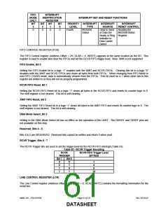
INTERRUPT ENABLE REGISTER (IER)
The lower four bits of the Interrupt Enable register (Address Offset = 1H, DLAB = 0, READ/WRITE) control the
enables of the five interrupt sources of the Serial Port interrupt. It is possible to totally disable the interrupt system by
resetting bits 0 through 3 of this register. Similarly, by setting the appropriate bits of this register to a high selected
interrupts can be enabled. Disabling the interrupt system inhibits the Interrupt Identification Register and disables any
Serial Port interrupt out of the FDC37N769. All other system functions operate in their normal manner, including the
Line Status and MODEM Status Registers. The contents of the Interrupt Enable Register are described below.
ERDAI, Bit 0
The ERDAI bit enables the Received Data Available Interrupt (and time-out interrupts in the FIFO mode) when set to
logic “1”.
ETHREI, Bit 1
The ETHREI bit enables the Transmitter Holding Register Empty Interrupt when set to logic “1”.
ELSI, Bit 2
The ELSI bit enables the Received Line Status Interrupt when set to logic “1”. The error sources causing the interrupt
are Overrun, Parity, Framing and Break. The Line Status Register must be read to determine the source.
EMSI, Bit 3
The EMSI bit enables the MODEM Status Interrupt when set to logic “1”. An MSI is caused when one of the Modem
Status Register bits changes state.
Reserved, Bits 4 - 7
Bits 4 to 7 are RESERVED. Reserved bits cannot be written and return 0 when read.
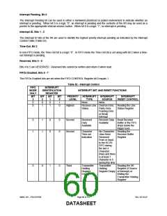
INTERRUPT IDENTIFICATION REGISTER (IIR)
By accessing the Interrupt Identification register (Address Offset = 2H, DLAB = X, READ), the host CPU can
determine the highest priority interrupt and its source. Four levels of interrupt priority exist. They are in descending
order of priority:
1. Receiver Line Status (highest priority)
2. Received Data Ready
3. Transmitter Holding Register Empty
4. MODEM Status (lowest priority)
Information indicating that a prioritized interrupt is pending and the source of that interrupt is stored in the Interrupt
Identification Register (refer to the Interrupt Control Table, Table 52). When the CPU accesses the IIR, the Serial
Port freezes all interrupts and indicates the highest priority pending interrupt to the CPU. During this CPU access,
even if the Serial Port records new interrupts, the current indication does not change until access is completed.
SMSC DS – FDC37N769
Page 59 of 137
Rev. 02-16-07
DATASHEET

 SMSC [ SMSC CORPORATION ]