COMPATIBILITY
The FDC37N769 was designed with software compatibility in mind. It is a fully backwards-compatible solution
with the older generation 765A/B disk controllers. The FDC also implements on-board registers for compatibility
with the PS/2, as well as PC/AT and PC/XT, floppy disk controller subsystems. After a hardware reset of the FDC, all
registers, functions and enhancements default to a PC/AT, PS/2 or PS/2 Model 30 compatible operating mode,
depending on how the IDENT and MFM bits are configured by the system BIOS.
Parallel Port Floppy Disk Controller
In this mode, the Floppy Disk Control signals are available on the parallel port pins. When this mode is selected, the
parallel port is not available. There are two modes of operation, PPFD1 and PPFD2. These modes can be selected
in Configuration Register 4. PPFD1 has only drive 1 on the parallel port pins; PPFD2 has drive 0 and 1 on the
parallel port pins.
PPFD1: Drive 0 is on the FDC pins
Drive 1 is on the Parallel port pins
PPFD2: Drive 0 is on the Parallel port pins
Drive 1 is on the Parallel port pins
When the PPFDC is selected the following pins are set as follows:
1. nDACK: Assigned to the parallel port device during configuration.
2. PDRQ (assigned to the parallel port): not ECP = high-Z, ECP & dmaEn = 0, ECP & not dmaEn = high-Z
3. IRQ assigned to the parallel port: not active, this is hi-Z or Low depending on settings.
The following parallel port pins are read as follows by a read of the parallel port register:
1. Data Register (read) = last Data Register (write)
2. Control Register are read as “cable not connected” STROBE, AUTOFD and SLC = 0 and nINIT = 1;
3. Status Register reads: nBUSY = 0, PE = 0, SLCT = 0, nACK = 1, nERR = 1.
The following FDC pins are all in the high impedance state when the PPFDC is actually selected by the drive select
register:
1. nWDATA, DENSEL, nHDSEL, nWGATE, nDIR, nSTEP, nDS1, nDS0, nMTRO, nMTR1.
2. If PPFDx is selected, then the parallel port can not be used as a parallel port until “Normal” mode is selected.
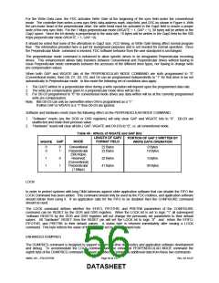
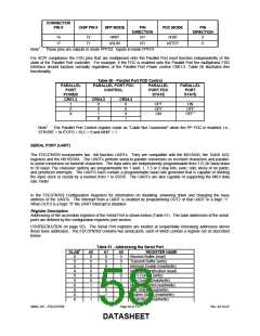
The FDC signals are muxed onto the Parallel Port pins as shown in Table 49.
Table 49 - FDC Parallel Port Pins
CONNECTOR
PIN #
CHIP PIN #
SPP MODE
PIN
FDC MODE
PIN
DIRECTION
DIRECTION
1
2
75
69
68
67
66
64
63
62
61
60
59
58
57
74
73
nSTB
PD0
I/O
I/O
I/O
I/O
I/O
I/O
I/O
I/O
I/O
I
(nDS0)
nINDEX
nTRK0
I/(0)1
I
I
I
I
I
3
PD1
4
PD2
nWP
5
PD3
nRDATA
nDSKCHG
6
PD4
7
PD5
8
PD6
(nMTR0)
I/(0) 1
9
PD7
10
11
12
13
14
15
nACK
BUSY
PE
nDS1
0
0
0
0
0
0
I
nMTR1
I
nWDATA
nWGATE
nDENSEL
nHDSEL
SLCT
nAFD
nERR
I
I/O
I
SMSC DS – FDC37N769
Page 57 of 137
Rev. 02-16-07
DATASHEET

 SMSC [ SMSC CORPORATION ]