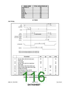
OPERATIONAL DESCRIPTION
MAXIMUM GUARANTEED RATINGS
Operating Temperature Range........................................................................................................................... 0oC to +70oC
Storage Temperature Range............................................................................................................................-55o to +150oC
Lead Temperature Range (soldering, 10 seconds)..................................................................................................... +325oC
Positive Voltage on any pin, with respect to Ground ......................................................................................................+5.5V
Negative Voltage on any pin, with respect to Ground......................................................................................................-0.3V
Maximum VCC.....................................................................................................................................................................+5V
*Stresses above those listed above could cause permanent damage to the device. This is a stress rating only and
functional operation of the device at any other condition above those indicated in the operation sections of this
specification is not implied.
Note: When powering this device from laboratory or system power supplies, it is important that the Absolute
Maximum Ratings not be exceeded or device failure can result. Some power supplies exhibit voltage spikes on their
outputs when the AC power is switched on or off. In addition, voltage transients on the AC power line may appear on
the DC output. If this possibility exists, it is suggested that a clamp circuit be used.
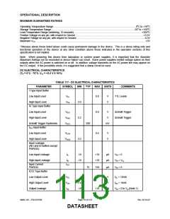
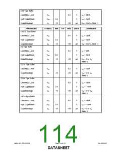
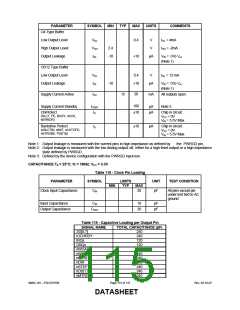
DC ELECTRICAL CHARACTERISTICS
(TA = 0°C - 70°C, Vcc = +3.3 V ± 10%)
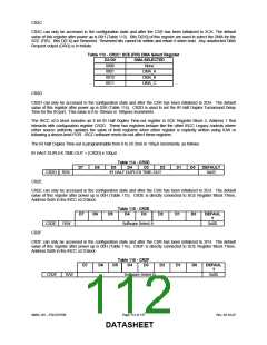
TABLE 117 - DC ELECTRICAL CHARACTERISTICS
PARAMETER
SYMBOL
MIN
TYP
MAX
UNITS
COMMENTS
I Type Input Buffer
Low Input Level
VILI
VIHI
0.8
V
V
TTL Levels
High Input Level
2.0
IS Type Input Buffer
Low Input Level
High Input Level
VILIS
VIHIS
VHYS
0.8
0.4
V
V
Schmitt Trigger
Schmitt Trigger
2.2
Schmitt Trigger Hysteresis
ICLK Input Buffer
250
mV
Low Input Level
VILCK
VIHCK
V
V
High Input Level
2.2
Input Leakage
(All I and IS buffers except
PWRGD)
Low Input Leakage
IIL
-10
-10
+10
+10
µA
µA
V
IN = 0
High Input Leakage
IIH
VIN = Vcc
Input Current
PWRGD
IOH
75
150
0.4
µA
V
IN = 0
IO12 Type Buffer
Low Output Level
High Output Level
Output Leakage
VOL
VOH
IOL
V
V
I
OL = 12mA
OH = -6mA
2.4
-10
I
+10
µA
VIN = 0 to Vcc (Note 1)
SMSC DS – FDC37N769
Page 113 of 137
Rev. 02-16-07
DATASHEET

 SMSC [ SMSC CORPORATION ]