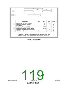
PARAMETER
O4 Type Buffer
SYMBOL MIN
TYP
MAX
UNITS
COMMENTS
Low Output Level
High Output Level
Output Leakage
VOL
0.4
V
V
I
OL = 4mA
OH = -2mA
VOH
IOL
2.4
-10
I
+10
µA
V
IN = 0 to Vcc
(Note 1)
OD12 Type Buffer
Low Output Level
Output Leakage
VOL
IOL
0.4
V
I
OL = 12 mA
-10
+10
µA
VIN = 0 to Vcc
(Note 1)
20
Supply Current Active
ICC
15
mA
All outputs open.
100
±10
Supply Current Standby
ICSBY
IIL
µA
µA
Note 3
ChiProtect
(SLCT, PE, BUSY, nACK,
nERROR)
Chip in circuit:
VCC = 0V
VIN = 5.5V Max.
Backdrive Protect
IIL
±10
µA
Chip in circuit:
(nSLCTIN, nINIT, nAUTOFD,
nSTROBE, PD[7:0])
V
CC = 0V
VIN = 5.5V Max.
Note 1: Output leakage is measured with the current pins in high impedance as defined by
the PWRGD pin.
Note 2: Output leakage is measured with the low driving output off, either for a high level output or a high impedance
state defined by PWRGD.
Note 3: Defined by the device configuration with the PWRGD input low.
CAPACITANCE TA = 25°C; fc = 1MHz; VCC = 3.3V
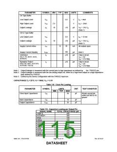
Table 118 - Clock Pin Loading
PARAMETER
SYMBOL
LIMITS
TYP
UNIT
TEST CONDITION
MIN
MAX
Clock Input Capacitance
CIN
20
pF
All pins except pin
under test tied to AC
ground
Input Capacitance
Output Capacitance
CIN
10
20
pF
pF
COUT
Table 119 - Capacitive Loading per Output Pin
SIGNAL NAME
SD[0:7]
IOCHRDY
IRQs
TOTAL CAPACITANCE (pF)
240
240
120
120
240
240
240
240
240
240
240
DRQs
nWGATE
nWDATA
nHDSEL
nDIR
nSTEP
nDS[1:0]
nMTR[1:0]
SMSC DS – FDC37N769
Page 115 of 137
Rev. 02-16-07
DATASHEET

 SMSC [ SMSC CORPORATION ]