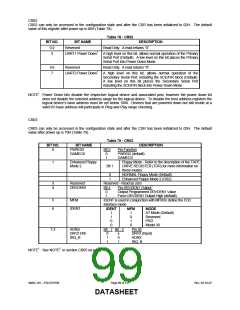
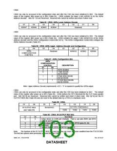
CR02
CR02 can only be accessed in the configuration state and after the CSR has been initialized to 02H. The default
value of this register after power up is 88H (Table 78).
Table 78 - CR02
BIT NO.
BIT NAME
Reserved
DESCRIPTION
0:2
3
Read Only. A read returns “0”.
UART1 Power Down1 A high level on this bit, allows normal operation of the Primary
Serial Port (Default). A low level on this bit places the Primary
Serial Port into Power Down Mode.
4:6
7
Reserved
Read Only. A read returns “0”.
UART2 Power Down1 A high level on this bit, allows normal operation of the
Secondary Serial Port, including the SCE/FIR block (Default).
A low level on this bit places the Secondary Serial Port
including the SCE/FIR block into Power Down Mode.
NOTE1: Power Down bits disable the respective logical device and associated pins, however the power down bit
does not disable the selected address range for the logical device. To disable the host address registers the
logical device’s base address must be set below 100h. Devices that are powered down but still reside at a
valid I/O base address will participate in Plug-and-Play range checking.
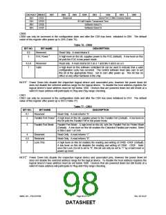
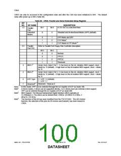
CR03
CR03 can only be accessed in the configuration state and after the CSR has been initialized to 03H. The default
value after power up is 70H (Table 79).
Table 79 - CR03
BIT NO.
BIT NAME
PWRGD/
GAMECS
DESCRIPTION
0
Bit 0
0
Pin Function
PWRGD (default)
1
GAMECS
1
Enhanced Floppy
Mode 2
Floppy Mode - Refer to the description of the TAPE
DRIVE REGISTER (TDR) for more information on
these modes.
Bit 1
0
1
NORMAL Floppy Mode (Default)
Enhanced Floppy Mode 2 (OS2)
3
4
Reserved
DRVDEN1
Reserved - Read as zero
Bit 4
0
Pin DRVDEN1 Output1
Output Programmed DRVDEN1 Value
Force DRVDEN1 Output High (default)
1
5
6
MFM
IDENT is used in conjunction with MFM to define the FDC
interface mode.
IDENT
IDENT
MFM
MODE
1
1
0
0
1
0
1
0
AT Mode (Default)
Reserved
PS/2
Model 30
7,2
ADRx/
Bit - 7 Bit - 2
Pin 92
DRV2 EN/
IRQ_B
0
1
1
x
0
1
DRV2 (Input)
ADRX
IRQ_B
NOTE1: See NOTE2 in section CR05 on page 101.
SMSC DS – FDC37N769
Page 99 of 137
Rev. 02-16-07
DATASHEET

 SMSC [ SMSC CORPORATION ]