Fan Control Device with Hardware Monitoring and Acoustic Noise Reduction Features
Datasheet
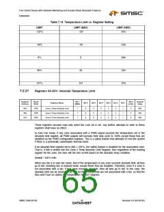
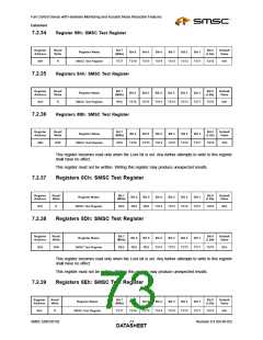
7.2.28
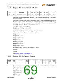
Register 7Eh: Interrupt Enable 1 Register
Register
Address
Read/
Write
Bit 7
Bit 0
Default
Value
Register Name
Bit 6
Bit 5
Bit 4
Bit 3
Bit 2
Bit 1
(MSb)
(LSb)
7Eh
R/W
Interrupt Enable 1 (Voltages)
VCC
12V
5V
RES
VCCP
25V
RES
VOLT
ECh
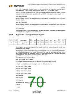
This register becomes read only when the Lock bit is set. Any further attempts to write to this register
shall have no effect.
This register is used to enable individual voltage error events to set the corresponding status bits in
the interrupt status registers. This register also contains the group voltage enable bit (Bit[0] VOLT),
which is used to enable voltage events to force the interrupt pin (INT#) low if interrupts are enabled
(see Bit[2] INTEN of the Special Function register at offset 7Ch).
This register contains the following bits:
Bit[0] Group INT# Voltage Enable (VOLT)
0=Out-of-limit voltages do not affect the state of the INT# pin (default)
1=Enable out-of-limit voltages to make the INT# pin active low
Bit[1] Reserved
Bit[2] 2.5V Error Enable
Bit[3] Vccp Error Enable
Bit[4] Reserved
Bit[5] 5V Error Enable
Bit[6] 12V Error Enable
Bit[7] VCC Error Enable
The individual voltage error event bits are defined as follows:
0=disable
1=enable.
See Figure 5.1 Interrupt Control on page 22.
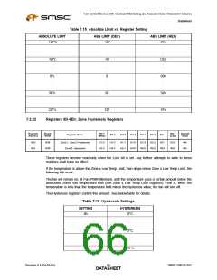
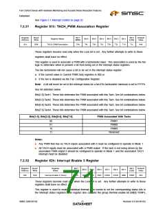
7.2.29
Register 7Fh: Configuration Register
Register
Address
Read/
Write
Bit 7
Bit 0
Default
Value
Register Name
Bit 6
Bit 5
Bit 4
Bit 3
Bit 2
Bit 1
(MSb)
(LSb)
7Fh
R/W
Configuration
INIT
SMSC
SMSC
SUREN
TRDY
RES
P2INT
T3INT
10h
These registers become read only when the Lock bit is set. Any further attempts to write to these
registers shall have no effect.
This register contains the following bits:
Bit[0] TACH3/INT# pin select: 0=TACH, 1=INT#
Bit[1] PWM2/INT# pin select: 0=PWM, 1=INT#
Bit[2] Reserved
SMSC EMC6D102
Revision 0.4 (04-05-05)
DATA6S9HEET

 SMSC [ SMSC CORPORATION ]