Fan Control Device with Hardware Monitoring and Acoustic Noise Reduction Features
Datasheet
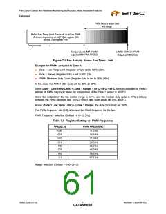
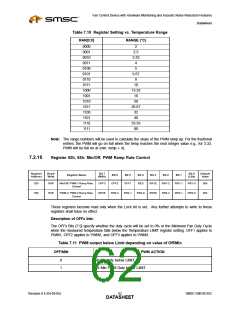
Table 7.10 Register Setting vs. Temperature Range
RAN[3:0]
RANGE (°C)
0000
0001
0010
0011
0100
0101
0110
0111
1000
1001
1010
1011
1100
1101
1110
1111
2
2.5
3.33
4
5
6.67
8
10
13.33
16
20
26.67
32
40
53.33
80
Note: The range numbers will be used to calculate the slope of the PWM ramp up. For the fractional
entries, the PWM will go on full when the temp reaches the next integer value e.g., for 3.33,
PWM will be full on at (min. temp + 4).
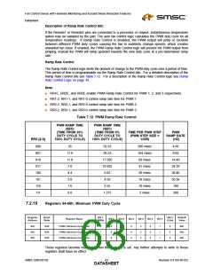
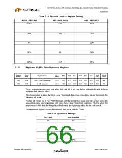
7.2.18
Register 62h, 63h: Min/Off, PWM Ramp Rate Control
Register
Address
Read/
Write
Bit 7
Bit 0
Default
Value
Register Name
Bit 6
Bit 5
Bit 4
Bit 3
Bit 2
Bit 1
(MSb)
(LSb)
62h
R/W
Min/Off, PWM 1 Ramp Rate
Control
OFF3
RR2E
OFF2
OFF1
RES
RR1E
RR1-2
RR1-1
RR1-0
RR3-0
00h
63h
R/W
PWM 2, PWM 3 Ramp Rate
Control
RR2-2
RR2-1
RR2-0
RR3E
RR3-2
RR3-1
00h
These registers become read only when the Lock bit is set. Any further attempts to write to these
registers shall have no effect.
Description of OFFx bits:
The OFFx Bits [7:5] specify whether the duty cycle will be set to 0% or the Minimum Fan Duty Cycle
when the measured temperature falls below the Temperature LIMIT register setting. OFF1 applies to
PWM1, OFF2 applies to PWM2, and OFF3 applies to PWM3.
Table 7.11 PWM output below Limit depending on value of Off/Min
OFF/MIN
PWM ACTION
0
1
At 0% duty below LIMIT
At Min PWM Duty below LIMIT
Revision 0.4 (04-05-05)
SMSC EMC6D102
DATA6S2HEET

 SMSC [ SMSC CORPORATION ]