Legacy-Free Keyboard/Embedded Controller with SPI and LPC Docking Interface
and the PLL_STOP bit changes from “1” to “0”, there is a delay of 100µs max. before the PLL clocks
are stable.
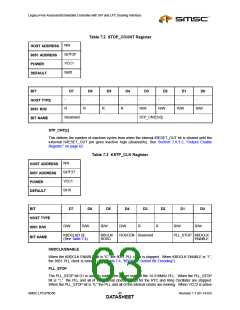
ROSCEN
This bit reflects the state of the ring oscillator clock at all times. The 8051 can write this bit to start or
stop the ring oscillator. Other hardware events can also start or stop this clock.
= 1 turn on ring oscillator
= 0 turn off ring oscillator
This bit is reset when the 8051 goes into “SLEEP” mode and is set when the 8051 first wakes up from
“SLEEP” mode.
Note 7.1 When VCC1 is active and the ROSCEN bit changes from “0” to “1”, there is a delay of 6 µs
max. before the ring oscillator starts.
KBCLK/ROSC
This bit is used to control the clock source for the 8051.
1 = 8051 clock source is KBCLK
0 = 8051 clock source is ring oscillator.
This bit is reset when the 8051 just wakes up from the “SLEEP” mode
KBDCLK[1:0]
These 2 bits control the 8051 system clock frequencies (See Table 7.4, "KBDCLK Control Bit
Encoding").
Table 7.4 KBDCLK Control Bit Encoding
KBDCLK[1:0] BITS (SEE Table 7.3)
KSTP_CLK REGISTER
KBD CLOCK FREQUENCIES
LPC47N350
D7 = KBDCLK[1]
D6 = KBDCLK[0]
0
0
1
0
1
12MHz
16MHz
24MHz
32MHz
1
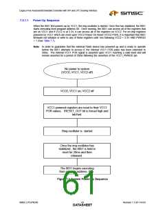
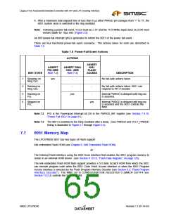
7.6
8051 Ring Oscillator Fail-Safe Controls
A fail-safe control for the 8051 ring oscillator protects against unpredicted VCC2 power failures. The
fail-safe ring oscillator sequence occurs as follows:
1. A VCC2 power-fail event is detected when the PWRGD pin changes from “1” to “0” (see Figure 2.1
on page 12).
2. The power-fail event sequence starts the 8051 Ring Oscillator. The Ring Oscillator frequency range
is 4MHz to 12MHz.
3. After a delay of 2.76µs max. the 8051 clock starts transitioning to the Ring Oscillator.
4. A smooth transition requires two ring clocks and two PPL clocks.
5. An additional 2 µs delay is incorporated to protect the rest of the chip.
Revision 1.1 (01-14-03)
SMSC LPC47N350
DATA4S6HEET

 SMSC [ SMSC CORPORATION ]