Legacy-Free Keyboard/Embedded Controller with SPI and LPC Docking Interface
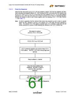
7.3.1.1
Power-Up Sequence
When the 8051 first powers up by VCC1, the ring oscillator is started. Once this has stabilized, the 8051
starts executing from program address 00. Once running, the 8051 can access all of the registers that
are on VCC1 and if VCC2 is at 3.3V, it can access all of the registers on VCC2. For on-chip registers
powered by VCC1 which are reset upon VCC2 Power On Reset (VCC2 POR), it is important that 8051
firmware not initialize or write to any of these registers until 1ms following VCC2 = 3.3V AND PWRGD
= 1 (See Table 7.7).
Note: In order to guarantee that the external Flash device has powered up and is ready to operate
before the 8051 attempts to access it, the internal VCC1 POR pulse has been extended to
20ms. The internal VCC1 POR signal is asserted upon VCC1 reaching a valid level and will
remain asserted for a period of 20ms following the assertion of the VCC1_PWRGD pin.
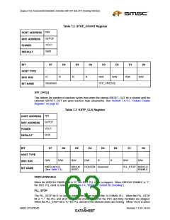
No power to system
(VCC0, VCC1, VCC2 off)
VCC0, VCC1 on; VCC2 off
VCC1 powered registers are reset to their VCC1
POR values. IRESET_OUT bit is forced high and
latched.
Ring oscillator is started
Once the ring oscillator has
stabilized , the 8051 is held in
reset for 20ms and then
released .
The 8051 begins executing
from program address 00h .
Figure 7.1 System Power-Up Sequence
SMSC LPC47N350
Revision 1.1 (01-14-03)
DATA4S3HEET

 SMSC [ SMSC CORPORATION ]