Legacy-Free Keyboard/Embedded Controller with SPI and LPC Docking Interface
Table 7.6 8051 Control Registers (continued)
SFR
REGISTER
VCC1
POR
NAME
ADDR
FIX BIT REGISTERS
D4 D3
EXF2 RCLK TCLK EXEN2
NOTE
D7
D6
D5
D2
D1
D0
T2CON
C8h
TF2
TR2
C/T2 CP/R
L2
Note 7.8
RCAP2L
RCAP2H
TL2
CAh
CBh
CCh
CDh
D0h
D8h
TH2
PSW
CY
AC
1
F0
RS1
PFI
RS0
OV
0
F1
0
P
0
Note 7.8
EICON
SMOD1
EPFI
WDTI
40h
E0h
E0h
Note 7.4
Note 7.8
ACC
EIE
E0h
E8h
Note 7.8
1
1
1
1
1
1
EWDI
PWDI
EX5
PX5
EX4
PX4
EX3
PX3
EX2
PX2
Note 7.4
Note 7.8
B
F0h
F8h
Note 7.8
EIP
Note 7.4
Note 7.8
Note 7.4 Not part of standard 8051 architecture.
Note 7.5 The MPAGE special function register provides a means of 16-bit addressing without using
the data pointer. During MOVX A, @Ri and MOVX @Ri, A instructions, the 8051 places the
contents of the MPAGE register on the upper 8 address bits. The MPAGE register default
is ‘00H’.
Note 7.6 The TM2 bit in the CKCON register is available, but not used, when Timer 2 is not
implemented (timer =0).
Note 7.7 Not part of standard 8051 architecture. Supports SPGIO[30:33]. See Section 20.5, "Bit-Wise
Addressable 8051 SFR GPIOs," on page 235.
Note 7.8 Bit-addressable register
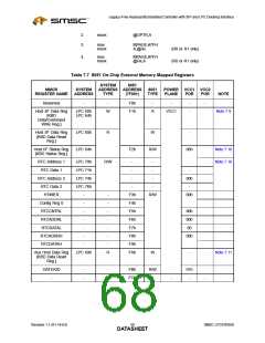
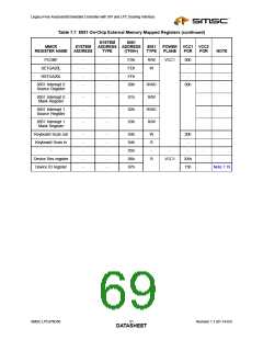
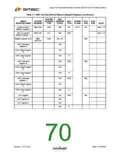
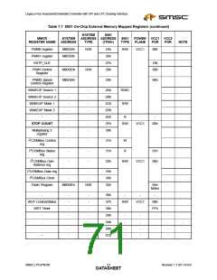
7.8.2
Memory Mapped Control Register (MMCR)
The Memory Mapped Control Registers are on-chip memory-mapped registers that can be accessed by
the 8051 but are external to the 8051 core (Table 7.7). The 8051 can access all of the Memory Mapped
Control Registers. The 8051 MMCR addresses are described in Column #4 (8051 ADDR) in Table 7.7.
Some MMCRs can also be accessed through the LPC Host interface (LPCxxh), the Mailbox Registers
interface (MBXxxh), the Embedded Controller Interface (ECI BASE), and the ACPI PM1 Block Interface
(PM1). These addresses are described in Column #2 (SYSTEM ADDRESS) in Table 7.7.
These Memory Mapped Control Registers can be accessed by the following types of 8051 instructions:
1.
movx
A,@DPTR
SMSC LPC47N350
Revision 1.1 (01-14-03)
DATA4S9HEET

 SMSC [ SMSC CORPORATION ]