Legacy-Free Keyboard/Embedded Controller with SPI and LPC Docking Interface
Table 7.1 High-Performance 8051 Implemented Features (continued)
FEATURE
VALUE
DESCRIPTION
Interrupts
11
The high-performance 8051 interrupt unit provides 11 interrupt
sources (see Table 7.15 on page 66).
7.2.1
Functional Blocks
Below are the functional blocks that the 8051 core has control of through its on-chip memory/mapped
external registers.
■
■
■
■
■
■
■
■
■
■
■
■
■
■
■
8042-Style Keyboard Controller Interface
Extended Interrupts
Power Management Functions
Direct Keyboard Scan Matrix (up to 128 keys)
Four channel PS/2 Interface
Dual I2C/SMBus Interface
LED controls
RTC CMOS RAM Access
24 General Purpose I/O (GPIO) pins
ACPI Embedded Controller (see Chapter 4)
PM1 Block
Four Pulse Width Modulators
Dual Fan Tachometer interface
Mailbox Register Interface
Serial Peripheral Interface (SPI)
7.2.2
High-Performance 8051 Cycle Timing and Instruction Set
The high-performance 8051 processor offers increased performance by executing instructions in a 4-
clock cycle, as opposed to the standard 8051. The shortened bus timing improves the instruction
execution rate for most instructions by a factor of three over the standard 8051 architectures.
Some instructions require a different number of instruction cycles on the high-performance 8051than
they do on the standard 8051. In the standard 8051, all instructions except for MUL and DIV take one
or two instruction cycles to complete. In the high-performance 8051 architecture, instructions can take
between one and five instructions to complete. The average speed improvement for the entire
instruction set is approximately 2.5X. See Table A.1, “Legend for Instruction Set Table,” on page 309 for
number of cycles on individual instruction requirements.
7.3
Powering Up or Resetting the 8051
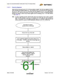
7.3.1
Default Reset Conditions
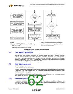
The LPC47N350 has two sources of reset: a VCC1 Power On Reset (VCC1 POR) or a VCC2 POR.
An LPC47N350 reset from any of these sources will cause the hardware response shown in Table 7.7,
"8051 On-Chip External Memory Mapped Registers". Note that the values shown are those prior to any
resident firmware control. Refer to Table 7.7 for the effect of each type of reset on each of the on-chip
registers.
Revision 1.1 (01-14-03)
SMSC LPC47N350
DATA4S2HEET

 SMSC [ SMSC CORPORATION ]