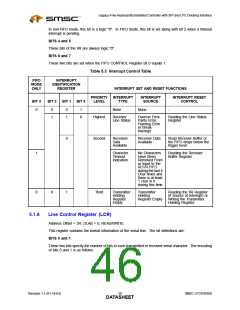
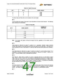
Legacy-Free Keyboard/Embedded Controller with SPI and LPC Docking Interface
BIT 1
Delta Data Set Ready (DDSR). This bit reads ‘0’.
BIT 2
Trailing Edge of Ring Indicator (TERI). This bit reads ‘0’.
BIT 3
Delta Data Carrier Detect (DDCD). This bit reads ‘0’
BIT 4
This bit is the complement of the Clear To Send (nCTS) input. This bit reads ‘0’.
BIT 5
This bit is the complement of the Data Set Ready (nDSR) input. This bit reads ‘0’.
BIT 6
This bit is the complement of the Ring Indicator (nRI) input. This bit reads ‘0’.
BIT 7
This bit is the complement of the Data Carrier Detect (nDCD) input. This bit reads ‘0’.
5.1.10 Scratchpad Register (SCR)
Address Offset =7H, DLAB =X, READ/WRITE
This 8 bit read/write register has no effect on the operation of the Serial Port. It is intended as a
Scratchpad register to be used by the programmer to hold data temporarily.
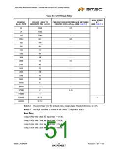
5.1.11 Programmable Baud Rate Generator (and Divisor Latches DLH, DLL)
The Serial Port contains a programmable Baud Rate Generator that is capable of dividing the internal
PLL clock by any divisor from 1 to 65535. The internal PLL clock is divided down to generate a
1.8462MHz frequency for Baud Rates less than 38.4k, a 1.8432MHz frequency for 115.2k, a 3.6864MHz
frequency for 230.4k and a 7.3728MHz frequency for 460.8k. This output frequency of the Baud Rate
Generator is 16x the Baud rate. Two 8 bit latches store the divisor in 16 bit binary format. These Divisor
Latches must be loaded during initialization in order to insure desired operation of the Baud Rate
Generator. Upon loading either of the Divisor Latches, a 16 bit Baud counter is immediately loaded.
This prevents long counts on initial load. If a 0 is loaded into the BRG registers, the output divides the
clock by the number 3. If a 1 is loaded, the output is the inverse of the input oscillator. If a two is
loaded, the output is a divide by 2 signal with a 50% duty cycle. If a 3 or greater is loaded, the output
is low for 2 bits and high for the remainder of the count. The input clock to the BRG is a 1.8462 MHz
clock.
Table 5.6 shows the baud rates possible.
Revision 1.1 (01-14-03)
SMSC LPC47N350
DATA3S2HEET

 SMSC [ SMSC CORPORATION ]