Legacy-Free Keyboard/Embedded Controller with SPI and LPC Docking Interface
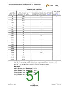
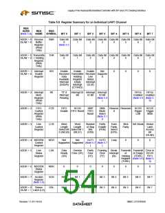
Table 5.8 Register Summary for an Individual UART Channel
REG
REG
ADDR
REG
(Note 5.4)
NAME
SYMBOL
BIT 0
BIT 1
BIT 2
BIT 3
BIT 4
BIT 5
BIT 6
BIT 7
ADDR = 0 Receive
RBR
Data Bit
0
Data Bit
1
Data Bit Data Bit Data Bit Data Bit Data Bit Data Bit
DLAB = 0
Buffer
Register
(Read
2
3
4
5
6
7
(Note 5.5
Only)
ADDR = 0 Transmitte
DLAB = 0 r Holding
Register
THR
IER
Data Bit
0
Data Bit
1
Data Bit Data Bit Data Bit Data Bit Data Bit Data Bit
2
3
4
5
6
7
(Write
Only)
ADDR = 1 Interrupt
DLAB = 0 Enable
Register
Enable
Enable
Enable
Not
0
0
0
0
Received Transmitter Receiver Supporte
Data
Holding
Register
Empty
Line
Status
Interrupt
(ELSI)
d
Available
Interrupt
(ERDAI)
Interrupt
(ETHREI)
ADDR = 2 Interrupt
Ident.
IIR
"0" if
Interrupt ID Interrupt Interrupt
FIFOs
FIFOs
Interrupt
Pending
Bit
ID Bit
ID Bit
(Note 5.9
)
Enabled Enabled
(Note 5.9 (Note 5.
9)
Register
(Read
Only)
ADDR = 2
ADDR = 3
FIFO
Control
Register
(Write
FCR
LCR
FIFO
RCVR
XMIT
FIFO
Reset
DMA
Mode
Select
(Note 5.1
0
Reserve Reserved
d
RCVR
Trigger
LSB
RCVR
Trigger
MSB
Enable FIFO Reset
Only)
Line
Word
Word
Number
of Stop
Bits
Parity
Enable
(PEN)
Even
Parity
Select
(EPS)
Stick
Set Break Divisor
Control
Register
Length
Length
Parity
Latch
Access
Bit
Select Bit Select Bit 1
0 (WLS0)
(WLS1)
(STB)
(DLAB)
ADDR = 4 MODEM
Control
MCR
LSR
Not
Not
OUT1
OUT2
Loop
0
0
0
Supported Supported (Note 5.7 (Note 5.7
Register
)
)
ADDR = 5
Line
Data
Ready
(DR)
Overrun
Parity
Error
(PE)
Framing
Error
Break Transmitt Transmitt Error in
Status
Error (OE)
Interrupt
(BI)
er
er Empty RCVR
(TEMT) FIFO
Register
(FE)
Holding
Register (Note 5.6) (Note 5.
(THRE)
0
9)
0
ADDR = 6 MODEM
Status
MSR
SCR
DDL
0
0
0
0
0
0
Register
ADDR = 7 Scratch
Register
Bit 0
Bit 0
Bit 1
Bit 1
Bit 2
Bit 2
Bit 3
Bit 3
Bit 4
Bit 4
Bit 5
Bit 5
Bit 6
Bit 6
Bit 7
Bit 7
(Note 5.8)
ADDR = 0 Divisor
DLAB = 1 Latch (LS)
Revision 1.1 (01-14-03)
SMSC LPC47N350
DATA3S6HEET

 SMSC [ SMSC CORPORATION ]