Legacy-Free Keyboard/Embedded Controller with SPI and LPC Docking Interface
Chapter 28 Electrical Specifications
28.1
Maximum Guaranteed Ratings*
Operating Temperature Range . . . . . . . . . . . . . . . . . . . . . . . . . . . . . . . . . . . . . . . . . . . . . . . 0 C to +70 C
o
o
o
o
Storage Temperature Range . . . . . . . . . . . . . . . . . . . . . . . . . . . . . . . . . . . . . . . . . . . . . . . .-55 to +150 C
o
Lead Temperature Range (soldering, 10 seconds) . . . . . . . . . . . . . . . . . . . . . . . . . . . . . . . . . . . . +325 C
Positive Voltage on any pin, with respect to Ground . . . . . . . . . . . . . . . . . . . . . . . . . . . . . . . . . . . . +5.5V
Negative Voltage on any pin, with respect to Ground . . . . . . . . . . . . . . . . . . . . . . . . . . . . . . . . . . . . 0.3V
Supply Voltage Range V 1 and V
2 . . . . . . . . . . . . . . . . . . . . . . . . . . . . . . . . . . . . . . . . . . . . .5 VDC
CC
CC
*Stresses above those listed above could cause permanent damage to the device. This is a stress
rating only and functional operation of the device at any other condition above those indicated in the
operation sections of this specification is not implied.
Note: When powering this device from laboratory or system power supplies, it is important that the
Absolute Maximum Ratings not be exceeded or device failure can result. Some power supplies
exhibit voltage spikes on their outputs when the AC power is switched on or off. In addition,
voltage transients on the AC power line may appear on the DC output. If this possibility exists,
it is suggested that a clamp circuit be used.
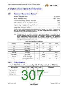
Table 28.1 Operating Conditions
SYMBOL
PARAMETER
MIN
TYP
MAX
UNITS
Vcc0
Vcc1
Vbat for RTC
Vcc for 8051
2.0
3.0
3.3
3.3
V
2.97
3.63
3.63
Vcc2
System Vcc
PCI_CLK
PCI Clock
33
MHz
kHz
MHz
°C
XTAL1/XTAL2
CLOCKI
RTC Crystal
32.768
14.318
14.318 Clock Input
Operating Temperature
T
0
70
A
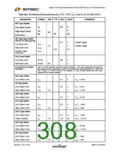
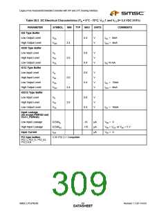
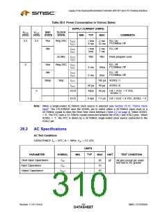
28.1.1 DC Specifications
Table 28.2 DC Electrical Characteristics (T = 0°C - 70°C, V 1 and V 2= 3.3 VDC ±10%)
A
CC
CC
PARAMETER
SYMBOL
MIN
TYP
MAX
UNITS
COMMENTS
I Type Input Buffer
Low Input Level
High Input Level
V
V
0.8
V
V
TTL Levels
IL
2.0
IH
SMSC LPC47N350
289
Revision 1.1 (01-14-03)
DATASHEET

 SMSC [ SMSC CORPORATION ]