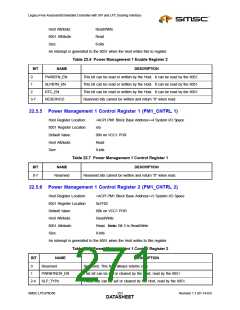
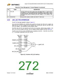
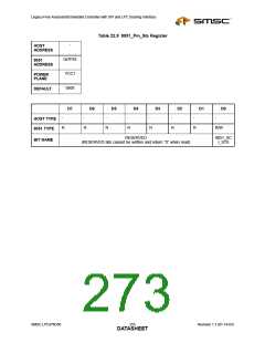
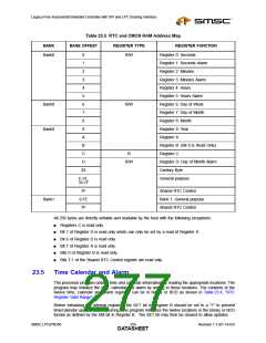
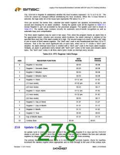
Legacy-Free Keyboard/Embedded Controller with SPI and LPC Docking Interface
Chapter 23 Real-Time Clock
23.1
General Description
The Real-Time Clock Supercell (RTC) is a complete time of day clock with alarm, day of month alarm,
one hundred year calendar, a century byte, and a programmable periodic interrupt. The RTC address
space consists of two-128 byte banks of CMOS RAM (Bank0 and Bank1). Each bank is accessable via
address and data ports. These access ports have relocatable addresses and are accessable by both
the host and the 8051. Each bank’s last addressable location accesses the Shared RTC Control. The
remaining 127 bytes of Bank0 contain the following: eleven registers of time, calendar, century, and
alarm data, four control and status registers, and 111 bytes of general purpose registers. The remaining
127bytes of Bank1 contain general purpose registers.
Features:
■
■
■
■
■
■
■
■
■
■
Allows 32kHz clock input or a 32kHz crystal.
Counts seconds, minutes, and hours of the day.
Counts days of the week, date, month and year.
Binary or BCD representation of time, calendar and alarm.
24 hour daily alarm.
30-day alarm.
RTC/CMOS Bank Addresses are relocatable.
The RTC CMOS Bank0 index register (70h) is shadowed
RTC Interrupt (IRQ8) is available on the parallel nIRQ8 pin.
RTC power source is switched internally between the VCC1 and VCC0 pins according to
VCC1_PWRGD (See Figure 2.2, "VCC2 Power-Up Timing" and Figure 2.3, "VCC1_PWRGD
Timing").
■
Lockable CMOS Ram Address Ranges (See Table 8.4 on page 90.
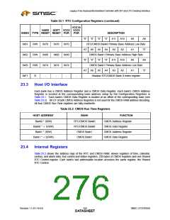
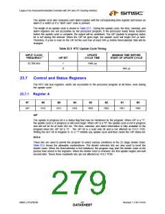
23.2
Configuration Registers
The RTC configuration registers, in Logical Device Number 6, provide activation control and the base
address for the run-time registers (See Table 23.1)
The activate bit register 0x30, Bit D0 enables RTC/CMOS Bank0.
The activate bit register 0x30, Bit D1 enables RTC/CMOS Bank1.
Table 23.1 RTC Configuration Registers
VCC1&
HARD
SOFT VCC2 VCC0
INDEX TYPE RESET RESET POR
POR
DESCRIPTION
D7 D6
D5
D4
D3
D2
D1
D0
0x30
0x60
R/W
R/W
0x00
0x00
0x00
0x00
0x00
0x00
-
Activate
RESERVED
Activate Activate
CMOS
Bank1
RTC/
CMOS
Bank0
-
RTC/CMOS Bank0 Primary Base Address High Byte
SMSC LPC47N350
257
Revision 1.1 (01-14-03)
DATASHEET

 SMSC [ SMSC CORPORATION ]