Legacy-Free Keyboard/Embedded Controller with SPI and LPC Docking Interface
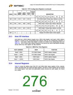
Table 23.1 RTC Configuration Registers (continued)
VCC1&
HARD
SOFT VCC2 VCC0
INDEX TYPE RESET RESET POR
POR
DESCRIPTION
“0” A11 A10
RTC/CMOS Bank0 Primary Base Address Low Byte
“0”
A7
“0”
A7
“0”
“0”
A9
A8
0x61
0x62
0x63
R/W
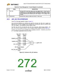
R/W
R/W
R
0x70
0x00
0x74
-
0x70
0x00
0x74
-
0x70
0x00
0x74
-
-
-
-
-
A6
CMOS Bank1 Primary Base Address High Byte
“0” “0” “0” A11 A10 A9
CMOS Bank1 Primary Base Address Low Byte
A6 A5 A4 A3 A2 A1
Shadow RTC/CMOS Bank 0 Index register
A5
A4
A3
A2
A1
“0”
A8
“0”
0xF1
23.3
Host I/O Interface
Each bank has a CMOS Address Register and a CMOS Data Register. Each bank’s CMOS Address
Register is located at the corresponding base address setup by the Configuration Registers in
Table 23.1. Each bank’s CMOS Data Register is located at an offset of the corresponding base (see
Table 23.2). Bit D7 of both CMOS Address Registers is not used for the CMOS RAM address decoding.
All four CMOS Run Time registers are fully read/write.
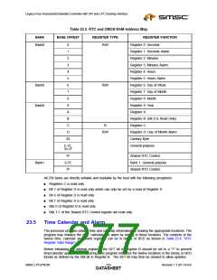
Table 23.2 CMOS Run Time Registers
HOST ADDRESS*
BANK
FUNCTION
Bank0 * (R/W)
Bank0 * + 1(R/W)
Bank1 * (R/W)
RTC/CMOS Bank0
RTC/CMOS Bank0
CMOS Bank1
CMOS Address Register
CMOS Data Register
CMOS Address Register
CMOS Data Register
Bank1 * + 2(R/W)
CMOS Bank1
23.4
Internal Registers
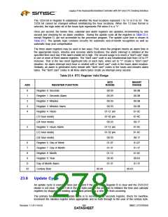
Table 23.3 shows the address map of the RTC and CMOS RAM, eleven registers of time, calendar,
century, and alarm data, four control and status registers, 239 bytes of CMOS registers and one Shared
RTC Control register. Each bank’s last addressable location accesses the same register, the Shared
RTC Control.
Revision 1.1 (01-14-03)
258
SMSC LPC47N350
DATASHEET

 SMSC [ SMSC CORPORATION ]