Legacy-Free Keyboard/Embedded Controller with SPI and LPC Docking Interface
Chapter 21 Multifunction Pin
21.1
Overview
Many of the LPC47N350’s signal pins provide alternate functions which may be enabled by the 8051
firmware based on the system design requirements. See Table 2.4 on page 10 for a complete list of all
of the multifunction pins. The 8051 firmware controls the multiplexing functions for each of the
multiplexed pins through the registers described in this section. See the sub-sections that follow for a
description of all of the MISC bits in the Multiplexing_1, Multiplexing_2, and Multiplexing_3 registers.
In the LPC47N350, the KBD Scan Interface Pins are multiplexed to support the 8051 Flash Interface.
The multiplex functions for these pins are not controlled by the 8051. For information about the
multiplexed KBD Scan Interface Pins see Section 9.6, "ATE Flash Program Access" and Section 9.7,
"External Flash Interface".
21.2
Functions Available on More than One Pin
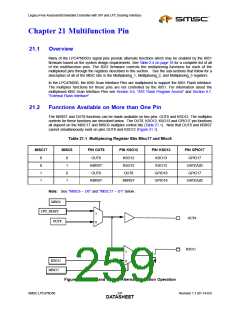
The KBRST and OUT8 functions can be made available on two pins: OUT8 and KSO12. The multiplex
controls for these functions are described below. The OUT8, KSO12, KSO13 and GPIO17 pin functions
all depend on the MISC17 and MISC6 multiplex control bits (Table 21.1). Note that OUT8 and KBRST
cannot simultaneously exist on pins OUT8 and KSO12 (Figure 21.1).
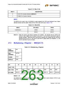
Table 21.1 Multiplexing Register Bits Misc17 and Misc6
MISC17
MISC6
PIN OUT8
PIN KSO12
PIN KSO13
PIN GPIO17
0
0
1
1
0
1
0
1
OUT8
KBRST
OUT8
KSO12
KSO12
OUT8
KSO13
KSO13
GPIO18
GPIO18
GPIO17
GATEA20
GPIO17
KBRST
KBRST
GATEA20
Note: See "MISC6 – D6" and "MISC17 – D1" below.
MISC6
CPU_RESET
1
0
OUT8
OUT8
KSO12
1
0
KSO12
MISC17
Figure 21.1 OUT8 and KSO12 Alternate Function Operation
SMSC LPC47N350
241
Revision 1.1 (01-14-03)
DATASHEET

 SMSC [ SMSC CORPORATION ]