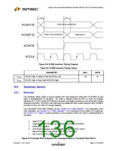
Legacy-Free Keyboard/Embedded Controller with SPI and LPC Docking Interface
Table 9.11 Exercising nDMS_LED Output Pin (continued)
PROCEDURE DESCRIPTION
ITEM #
2
Wait for the DMS_OVERFLOW bit to be asserted. When the DMS_DISABLE bit is deasserted,
the DMS counter will resume until overflow.
When the DMS_OVERFLOW bit is asserted,
the nDMS_LED output pin should begin
pulsing as shown in Figure 9.11.
3
4
Assert the DMS_DISABLE bit.
Assert the DMS_TEST bit.
Permanently disable the DMS counter.
Provide some means to signal the end of the
nDMS_LED test.
When the nDMS_LED test is complete, the
nDMS_LED output pin is permanently
deasserted when the DMS_TEST bit is
asserted.
5
Deassert the DMS_OVERFLOW bit.
Remove indication that the DMS overflow
state has been reached.
9.9.4.3
DMS_DISABLE Bit – D0
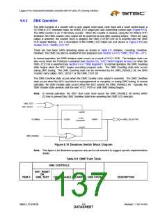
The DMS_DISABLE bit D0 is used to permanently stop the DMS counter (Figure 9.10). When the
DMS_DISABLE bit is deasserted ‘0’ (default), the DMS counter is enabled and will begin counting until
the DMS overflow state is reached, assuming the DMS_TEST bit and the 8051_RESET signal are
deasserted. When the DMS_DISABLE bit is asserted ‘1’, the DMS counter is permanently disabled. The
DMS_DISABLE bit can be used along with the DMS_TEST bit to exercise the nDMS_LED output pin
(see Section 9.9.4.2, "DMS_TEST Bit – D1" above).
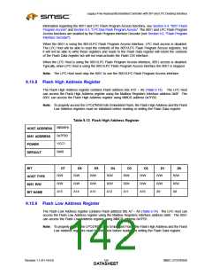
9.10
Flash Program Register
The Flash Program register contains the Flash Program Interface Decoder controls (see Section 9.2,
"Flash Program Interface Decoder") and the RESET FLASH control.
The Flash Program register is shown in Table 9.12. The Flash Program register is always available to
the LPC Host and to the 8051.
Table 9.12 Flash Program Register
MBX9Eh
0x7F35
HOST ADDRESS
8051 ADDRESS
POWER
VCC1
‘000XXX00’b
DEFAULT
BIT
D7
D6
D5
D4
D3
D2
D1
R/W
D0
R/W
R/W
R
R
R
R
R
R
R
R
R
HOST TYPE
8051 R/W
R/W
R
R/W
R/W
RESET
FLASH
Reserved
FWP
PIN
EXT
ATE
LPC
8051
PGM
BIT NAME
FLASH
PGM
PGM
Revision 1.1 (01-14-03)
122
SMSC LPC47N350
DATASHEET

 SMSC [ SMSC CORPORATION ]