Legacy-Free Keyboard/Embedded Controller with SPI and LPC Docking Interface
9.11
Scratch ROM
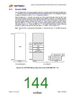
The LPC47N350 8051 can execute program code from a 512-byte Scratch ROM when the MMC bit is
‘1’. The MMC bit is D3 in CONFIGURATION REGISTER 0 (MMCR 0x7FF4). The Configuration Register
0 register is described in Section 7.8.3.4, "Configuration Register").
When the MMC bit is ‘1’, the 8051 can execute out of the Scratch ROM either when the 8051 Code
Fetch Access interface or when the 8051 Program Access interface is selected. For example, the 8051
can execute code from the Scratch ROM even when the 8051 Code Fetch Interface is unselected by
the Flash Program Interface Decoder (see Section 9.2, "Flash Program Interface Decoder" above).
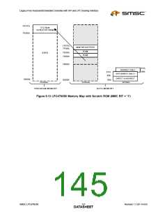
When the MMC bit = ‘0’, there is 512 bytes of Scratch RAM located at address 0x7B00 in the 8051
Data Space (Figure 9.12). When the MMC bit is ‘1’, the Scratch RAM becomes Scratch ROM and
occupies 512 bytes at the top of the 64k code space; i.e., FE00h – FFFFh (Figure 9.13).
Note: When the 8051 is running from external flash, i.e. when the nEA pin = ‘0’, the MMC bit must be
‘0’.
FFFFh
7FFFh
7F00h
M/M REGISTERS
RAM
64KB
7E00h
7D00h
RAM
512-Byte
SCRATCH RAM
7B00h
FFh
80h
INDIRECT ONLY
FFh
80h
SFR (DIRECT ONLY)
DIRECT & INDIRECT
INTERNAL
0000h
0000h
00h
EXTERNAL
EXTERNAL
PROGRAM MEMORY
DATA MEMORY
Figure 9.12 LPC47N350 Memory Map with Scratch RAM (MMC BIT = '0')
Revision 1.1 (01-14-03)
126
SMSC LPC47N350
DATASHEET

 SMSC [ SMSC CORPORATION ]