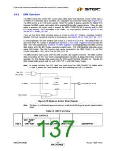
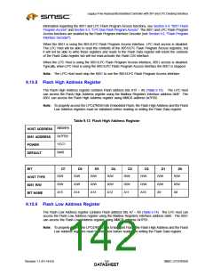
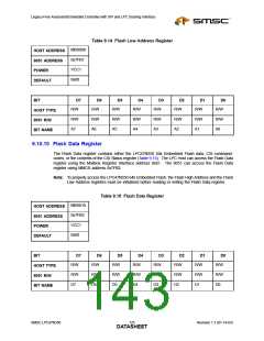
Legacy-Free Keyboard/Embedded Controller with SPI and LPC Docking Interface
9.10.1 RESET FLASH – D7
The RESET FLASH bit can reset the internal 64k Embedded Flash ROM (see Section 8.3.3, "Reset").
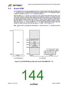
When the RESET FLASH bit is asserted ‘1’, the 64k Embedded Flash ROM is placed in a reset state.
When the RESET FLASH bit is de-asserted ‘0’ (default), the 64k Embedded Flash ROM is placed in
Read Array mode.
Note: The RESET FLASH bit is not self-clearing.
9.10.2 FWP – D4
The FWP Pin bit reflects the status of the nFWP input pin. When nFWP is asserted (‘0’), the boot block
in the LPC47N350 Embedded 64K Flash ROM is write-protected and the FWP Pin bit is asserted ‘1’.
When the nFWP pin is deasserted (‘1’), the boot block is writeable and the FWP Pin bit is deasserted ‘0’.
Note: The EXT FLASH bit is read-only and not affected by VCC1 POR.
9.10.3 EXT FLASH – D3
The EXT FLASH bit in the Flash Program register indicates the state of the LPC47N350 nEA pin. When
the nEA pin is asserted ‘0’, the EXT FLASH bit is asserted ‘1’, when the nEA pin is deasserted ‘1’, the
EXT FLASH bit is deasserted ‘0’. When the EXT FLASH bit is asserted (‘1’), the LPC47N350 Flash
programming interface is disabled (see Table 9.1).
9.10.4 ATE PGM – D2
The ATE PGM bit in the Flash Program register directly reflects the state of the LPC47N350 PGM pin.
When the PGM pin is asserted, the ATE PGM bit is asserted, when the PGM pin is deasserted, the ATE
PGM bit is deasserted. When the ATE PGM bit is asserted (‘1’), the LPC47N350 Flash programming
interface is dedicated to the ATE Flash Program Access function (see Table 9.1 and Section 9.6, "ATE
Flash Program Access" above).
Note: The ATE PGM bit is read-only and not affected by VCC1 POR.
9.10.5 LPC PGM – D1
The LPC PGM bit in the Flash Program register is used to enable the LPC Flash Program Access
function (see Table 9.1 and Section 9.5, "LPC Bus Flash Program Access", above). The LPC PGM bit
can only be asserted when the ATE PGM and the 8051 PGM bits are deasserted ‘0’ (Table 9.1), and
the SYSTEM FLASH bit in the Disable register is deasserted. When the LPC PGM bit is asserted ‘1’,
the LPC47N350 64k Embedded Flash is dedicated to the LPC Host programming interface. The LPC
PGM bit is read/write and deasserted by VCC1 POR.
9.10.6 8051 PGM – D0
The 8051 PGM bit in the Flash Program register is used to enable the 8051 Program Access function
(see Table 9.1 and Section 9.3, "8051 Code Fetch Access" above). The 8051 PGM bit can only be
asserted when the ATE PGM bit is deasserted ‘0’; the 8051 PGM bit overrides the LPC PGM bit
(Table 9.1).
When the 8051 PGM bit is asserted ‘1’, the 64k Embedded Flash is dedicated to the 8051 programming
interface. The 8051 PGM bit is read/write and deasserted by VCC1 POR.
9.10.7 8051/LPC Flash Program Access Registers
The 8051/LPC Flash Program Access registers are used by the 8051 and the LPC Host to program the
LPC47N350 64k Embedded Flash (see Figure 9.2 on page 110). To the 8051, the 8051/LPC Flash
Program Access registers are accessed using memory-mapped control registers; to the LPC host, the
8051/LPC Flash Program Access registers are accessed using the Mailbox Registers Interface. For
SMSC LPC47N350
123
Revision 1.1 (01-14-03)
DATASHEET

 SMSC [ SMSC CORPORATION ]