Legacy-Free Keyboard/Embedded Controller with SPI and LPC Docking Interface
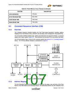
ROM address bus and the Flash Memory Array Main Memory addressing is shown below in Table 8.3.
The relationship between the 64k Embedded Flash ROM address bus and the Flash Memory Array
Information block addressing is shown below in Table 8.4. The upper seven host address bits A15 –
A9 determine the Flash page, the next three lower address bits A8 – A6 determine the row and the least
significant six bits determine the byte.
Table 8.3 Main Memory- 64K Embedded Flash Address Mapping
FLASH ADDRESS
A15
A14
A13 A12
A11
A10
A9
A8
A7
A6
A5
A4
A3
A2
A1
A0
A0
PAGES
ROWS
BYTES
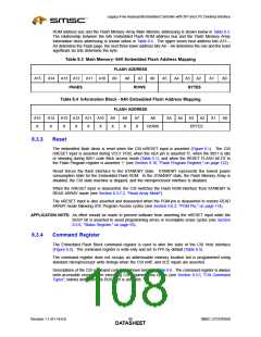
Table 8.4 Information Block - 64K Embedded Flash Address Mapping
FLASH ADDRESS
A15
X
A14
X
A13 A12 A11 A10
A9
X
A8
X
A7
X
A6
A5
A4
A3
A2
A1
X
X
X
X
ROWS
BYTES
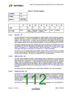
8.3.3
Reset
The embedded flash block is reset when the CSI nRESET input is asserted (Figure 8.1). The CSI
nRESET input is asserted during VCC1 POR, when the nEA pin is asserted ‘0’, when the 8051 is idle
or sleeping during 8051 code fetch access mode (Table 2.1), and when the RESET FLASH bit D7 in
the Flash Program register is asserted ‘1’ (see Section 9.10, "Flash Program Register," on page 122).
Reset forces the flash interface to the STANDBY state. STANDBY represents the lowest power
consumption state for the Embedded Flash ROM. In the STANDBY state, the Flash Memory Array is
disabled, the CSI state machine is stopped, and the microprocessor interface is disabled.
When the nRESET input is deasserted, the CSI switches the Flash ROM interface from STANDBY to
READ ARRAY mode (see Section 8.3.7.2, "Read Array Mode").
The nRESET input is also asserted and deasserted when the PGM pin is deasserted to restore READ
ARRAY mode following ATE Program Access cycles (see Section 9.6.3, "PGM Pin," on page 114).
APPLICATION NOTE: An effort should be made to prevent software from asserting the nRESET input while the
BUSY bit is asserted to avoid programming errors or incomplete erase cycles (see Section
8.3.6, "Status Register," on page 93).
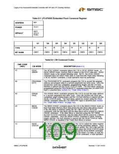
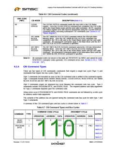
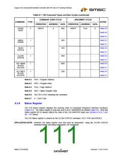
8.3.4
Command Register
The Embedded Flash Block command register is used to alter the state of the CSI Host Interface
(Figure 8.2). The command register is write-only and set to FFh by default (Table 8.5).
The command register does not occupy an addressable memory location but is programmed using
standard microprocessor write timings when the CSI nWE and nCE inputs are asserted.
Descriptions of the CSI command codes are shown below in Table 8.6. The command register is always
write-accessible except when executing CSI argument bus cycles (see Section 8.3.5, "CSI Command
Types", below) and when the BUSY bit is asserted.
Revision 1.1 (01-14-03)
SMSC LPC47N350
DATA9S0HEET

 SMSC [ SMSC CORPORATION ]