Legacy-Free Keyboard/Embedded Controller with SPI and LPC Docking Interface
Chapter 8 64K Embedded Flash ROM
8.1
Overview
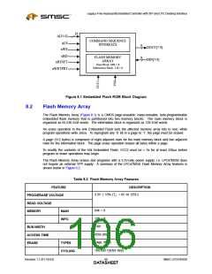
The LPC47N350 includes a 64k embedded Flash ROM (Figure 8.1). The embedded Flash ROM
consists of two basic components: a Flash Memory Array and a Command Sequence Interface (CSI).
The LPC47N350 Flash ROM stores the 8051-specific embedded keyboard/system controller runtime
code.
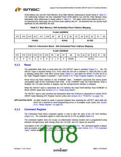
The memory arrangement of the LPC47N350 64k embedded Flash ROM includes a Main memory block
and an Information block. The bottom 2k of the Main Memory block (0x000 – 0x7FF), i.e. the boot block,
can be locked by the write-protect pin nFWP.
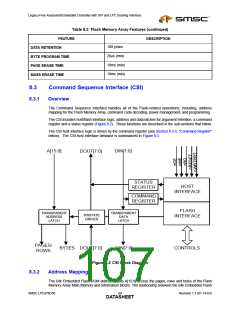
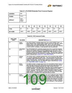
All read, program and erase operations in the LPC47N350 embedded Flash ROM can be controlled by
means of specific command sequences that can be written to the Flash ROM using standard
microprocessor write timings.
The LPC47N350 embedded Flash ROM can be directly programmed by the 8051. The Flash ROM can
also be programmed independently, i.e. without 8051 intervention, by both the LPC host through the
LPC Bus interface and externally using the keyboard scan interface pins.
Note: The Following Specifications Are Preliminary And Subject To Change.
Characteristics of the 64k embedded Flash ROM are summarized in Table 8.1:
Table 8.1 LPC47N350 64K Embedded Flash ROM Feature Summary
FEATURE
DESCRIPTION
3.3V ± 10% (TJ = 0×C to 125×C)
PROG/ERASE VOLTAGE
READ VOLTAGE
BUS WIDTH
8-bit
45 ns
ACCESS TIME
64k x 8
MAIN BLOCK
INFO. BLOCK
SIZE
MEMORY
ARRANGEMENT
128k x 8
2K-Byte, Lockable
Bottom
BOOT BLOCK
ERASE
LOCATION
TYPES
Page/Mass (512 bytes/page)
100,000 Cycles (Commercial Temp).
Per Byte
CYCLING
PROGRAMMING
INTERFACE
All Program and Erase Operations are Enabled via a Command
Sequence Interface using Standard Microprocessor Write Timings.
SMSC LPC47N350
Revision 1.1 (01-14-03)
DATA8S7HEET

 SMSC [ SMSC CORPORATION ]