Legacy-Free Keyboard/Embedded Controller with SPI and LPC Docking Interface
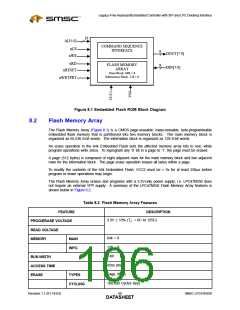
Table 8.2 Flash Memory Array Features (continued)
FEATURE DESCRIPTION
100 years
20µs (min)
10ms (min)
10ms (min)
DATA RETENTION
BYTE PROGRAM TIME
PAGE ERASE TIME
MASS ERASE TIME
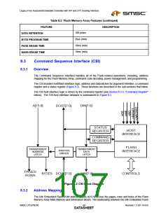
8.3
Command Sequence Interface (CSI)
8.3.1
Overview
The Command Sequence Interface handles all of the Flash-related operations; including, address
mapping for the Flash Memory Array, command code decoding, power management, and programming.
The CSI includes host/flash interface logic, address and data latches for argument retention, a command
register and a status register (Figure 8.2). These functions are described in the sub-sections that follow.
The CSI host interface logic is driven by the command register (see Section 8.3.4, "Command Register"
below). The CSI host interface behavior is summarized in Figure 8.3.
A[15:0]
DIN[7:0]
DOUT[7:0]
STATUS
HOST
INTERFACE
REGISTER
COMMAND
REGISTER
FLASH
INTERFACE
TRANSPARENT
ADDRESS
LATCH
TRANSPARENT
DATA
TRISTATE
DRIVER
LATCH
PAGES/
ROWS
BYTES DOUT[7:0]
DIN[7:0]
CONTROLS
Figure 8.2 CSI Block Diagram
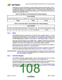
8.3.2
Address Mapping
The 64k Embedded Flash ROM address inputs A[15:0] access the pages, rows and bytes of the Flash
Memory Array Main Memory and Information blocks. The relationship between the 64k Embedded Flash
SMSC LPC47N350
Revision 1.1 (01-14-03)
DATA8S9HEET

 SMSC [ SMSC CORPORATION ]