Legacy-Free Keyboard/Embedded Controller with SPI and LPC Docking Interface
16
A[15:0]
COMMAND SEQUENCE
nCE
INTERFACE
8
8
DOUT[7:0]
DIN[7:0]
nWE
nRD
FLASH MEMORY
ARRAY
nRESET
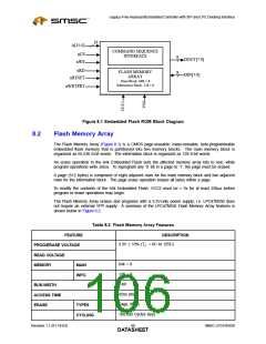
Main Block: 64K × 8
Information Block: 128 × 8
nWRTPRT
Figure 8.1 Embedded Flash ROM Block Diagram
8.2
Flash Memory Array
The Flash Memory Array (Figure 8.1) is a CMOS page-erasable, mass-erasable, byte-programmable
embedded flash memory that is partitioned into two memory blocks. The main memory block is
organized as 65,536 8-bit words. The information block is organized as 128 8-bit words.
An erase operation in the 64k Embedded Flash sets the affected memory array bits to one, while
program operations write zeros. To reprogram any ‘0’ bit in a page to ‘1’, the page must be erased.
A page (512 bytes) is composed of eight adjacent rows for the main memory block and two adjacent
rows for the information block. The page erase operation erases all bytes within a page.
To modify the contents of the 64k Embedded Flash, VCC2 must be > 3v for at least 250µs before
program or erase operations may begin.
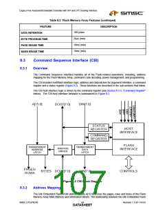
The Flash Memory Array erases and programs with a 3.3V-only power supply; i.e. LPC47N350 does
not require an external VPP supply. A summary of the LPC47N350 Flash Memory Array features is
shown below in Figure 8.2.
Table 8.2 Flash Memory Array Features
FEATURE
DESCRIPTION
3.3V ± 10% (TJ = 0C to 125C)
PROG/ERASE VOLTAGE
READ VOLTAGE
64k × 8
MEMORY
MAIN
128 × 8
INFO.
8-bit
BUS-WIDTH
ACCESS TIME
ERASE
45ns (max)
Page, Mass
100,000 Cycles (typ)
TYPES
CYCLING
Revision 1.1 (01-14-03)
SMSC LPC47N350
DATA8S8HEET

 SMSC [ SMSC CORPORATION ]