ST7565S
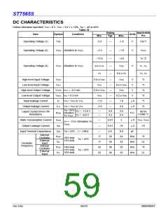
Table 19
Condition
Rating
Typ.
Applicable
Pin
Item
Symbol
Units
Min.
Max.
Input voltage
V
SS2
(Relative To VDD
)
–3.3
—
–1.8
V
V
VSS2
Supply Step-up output
voltage Circuit
Voltage regulator
Circuit Operating
Voltage
V
V
OUT (Relative To VDD
OUT (Relative To VDD
)
–16.0
–16.0
—
—
V
V
OUT
)
)
—
–6.0
V
OUT
Voltage Follower
Circuit Operating
Voltage
V
5
(Relative To VDD
–13.0
–2.07
—
–4.0
V
V
V5 * 9
Ta = 25°C , (Relative To V DD
–0.05%/°C
)
Base Voltage
V
RS
–2.10
–2.13
*10
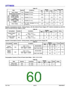
Dynamic Consumption Current : During Display, with the Internal Power Supply OFF Current consumed by total ICs
when an external power supply is used .
Table 20
Rating
Test pattern
Symbol
Condition
Units
Notes
Min.
Typ.
Max.
Display Pattern
OFF
VDD = 3.0 V,
V5 – VDD = –11.0 V
μA
—
16
27
*11
I
I
DD
DD
Display Pattern
Checker
VDD = 3.0 V,
V5 – VDD = –11.0 V
μA
—
19
32
*11
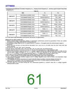
Dynamic Consumption Current : During Display, with the Internal Power Supply ON
Table 21
Rating
Typ.
Test pattern Symbol
Condition
Units Notes
Min.
Max.
Normal Mode
—
60
100
VDD = 3.0 V,
Quad step-up voltage.
V5 – VDD = –11.0 V
Display
Pattern OFF
μA
*12
I
I
DD
DD
High-Power Mode
—
—
—
98
70
163
Display
Pattern
Checker
Normal Mode
117
175
VDD = 3.0 V,
Quad step-up voltage.
V5 – VDD = –11.0 V
μA
*12
High-Power Mode
105
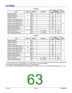
Consumption Current at Time of Power Saver Mode : VSS = -3.0 V ± 10%
Table 22
Rating
Typ.
0.1
Item
Symbol
Condition
Units
μA
Notes
Min.
Max.
Sleep mode
Ta = 25°C
Ta = 25°C
—
4
IDD
DD
Standby Mode
—
5
10
I
Ver 0.6c
60/72
2009/09/07

 SITRONIX [ SITRONIX TECHNOLOGY CO., LTD. ]