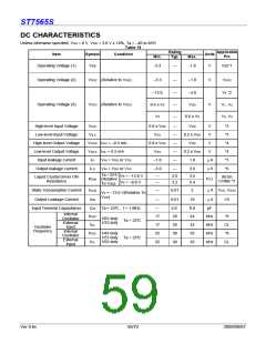
ST7565S
DC CHARACTERISTICS
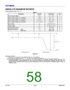
Unless otherwise specified, VSS = 0 V, VDD = 3.0 V ± 10%, Ta = –40 to 85°C
Table 18
Rating
Typ.
Applicable
Pin
Item
Symbol
Condition
Units
Min.
Max.
Operating Voltage (1)
Vss
-3.3
—
-1.8
V
Vss*1
Operating Voltage (2)
V
SS2 (Relative to VDD
)
)
–3.3
—
–1.8
–4.0
V
VSS2
–13.0
—
—
—
V5 *2
Operating Voltage (3)
V
SS2 (Relative to VDD
0.4 x V
5
V
DD
V
V
1
, V
, V
2
V
5
0.6 x V
5
V
3
4
High-level Input Voltage
Low-level Input Voltage
High-level Output Voltage
Low-level Output Voltage
Input leakage current
V
IHC
ILC
OHC
OLC
LI
LO
0.8 x VDD
—
—
—
—
—
—
V
DD
V
V
*3
*3
*4
*4
*5
*6
V
V
SS
0.2 x VDD
V
I
OH = –0.5 mA
OL = 0.5 mA
0.8 x VDD
V
DD
V
V
I
V
SS
0.2 x VDD
1.0
V
μA
μA
I
V
V
IN = VDD or VSS
IN = VDD or VSS
–1.0
–3.0
Output leakage current
I
3.0
Ta = 25°C
(Relative
V
V
5
5
= –13.0 V
= –8.0 V
—
—
2.0
3.2
3.5
5.4
Liquid Crystal Driver ON
Resistance
SEGn
COMn *7
KΩ
RON
To VDD
)
μA
μA
Static Consumption Current
I
SSQ
—
0.01
2
V
SS, VSS2
V5
V
V
5 = –13.0 V(Relative To
DD
)
Output Leakage Current
I
5Q
IN
OSC
CL
—
—
0.01
5.0
20
10
8.0
24
24
35
35
Input Terminal Capacitance
C
Ta = 25°C , f = 1 MHz
pF
Internal
Oscillator
External
f
17
17
25
25
kHz
kHz
kHz
kHz
*8
CL
*8
1/65 duty
Ta = 25°C
1/33 duty
f
20
Oscillator
Frequency
Input
Internal
Oscillator
External
Input
f
OSC 1/49 duty
1/53 duty Ta = 25°C
1/55 duty
30
f
CL
30
CL
Ver 0.6c
59/72
2009/09/07

 SITRONIX [ SITRONIX TECHNOLOGY CO., LTD. ]